 ALLPCB


If you're looking to design a printed circuit board (PCB) for wave soldering, you’re in the right place. Wave soldering is a widely used process for assembling through-hole components, and proper PCB design is critical to ensure reliable solder joints and high manufacturing yields. In this comprehensive guide, we’ll cover the essentials of wave soldering PCB design rules, including component orientation, pad design for through-hole parts, and thermal considerations. Let’s dive into the best practices to optimize your PCB for this soldering method.
What is Wave Soldering and Why Does PCB Design Matter?
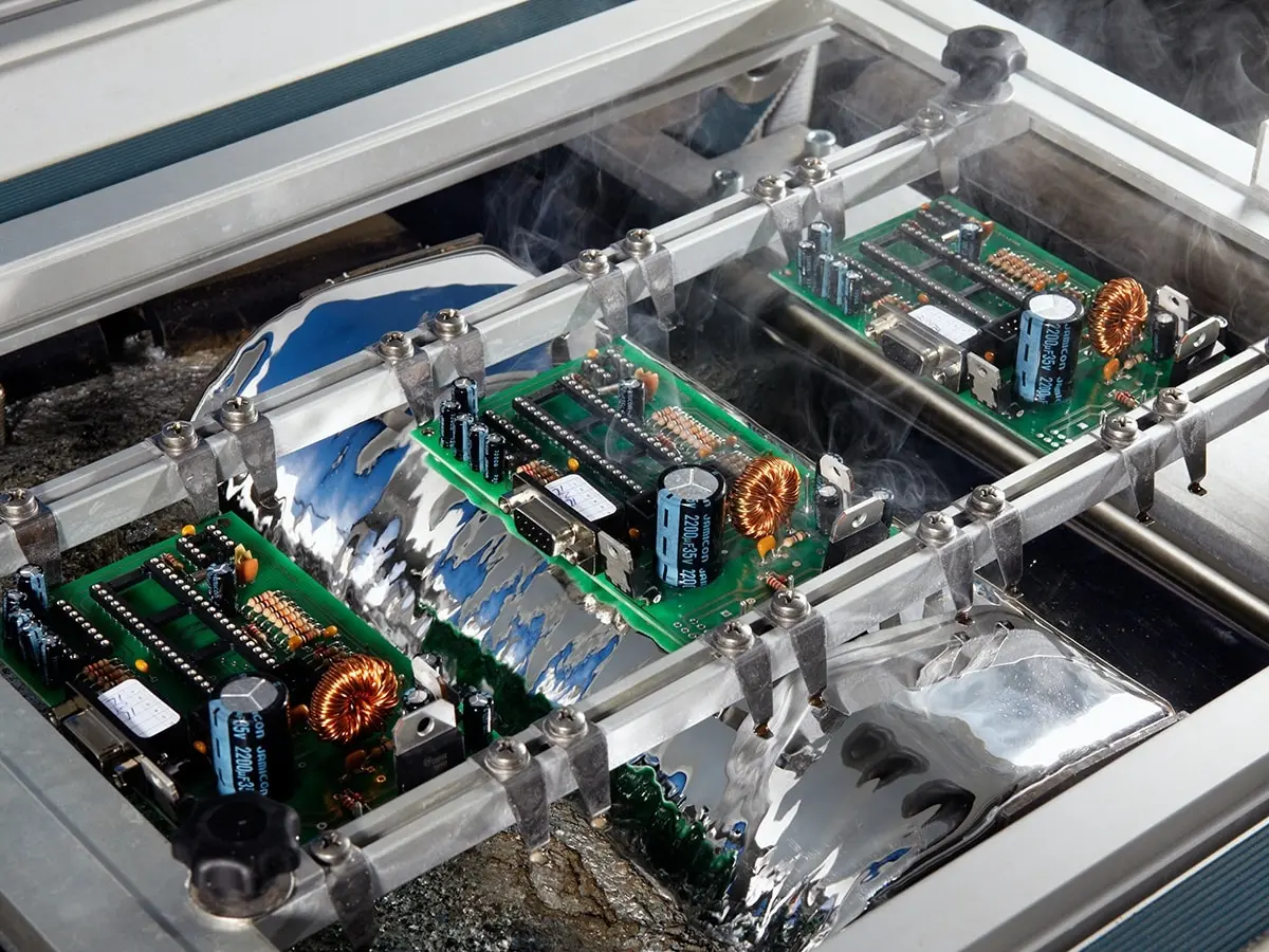
Wave soldering is a bulk soldering process used primarily for through-hole components on PCBs. During this process, the bottom side of the PCB passes over a wave of molten solder, which creates strong electrical and mechanical connections between component leads and the board. While efficient for high-volume production, wave soldering can lead to issues like solder bridging, insufficient solder joints, or component damage if the PCB isn’t designed with the process in mind.
Designing a PCB for wave soldering involves careful planning of component placement, pad design, and thermal management. A well-thought-out design reduces defects, improves reliability, and ensures the final product meets quality standards. Whether you're an experienced engineer or new to PCB design, following these wave soldering PCB design rules will help you achieve better results.
Key Wave Soldering PCB Design Rules
Designing a PCB for wave soldering requires attention to several critical factors. Below, we break down the most important rules to follow for a successful design.
1. Component Placement and Orientation for Wave Soldering
Component placement and orientation are crucial for ensuring even solder distribution and minimizing defects during wave soldering. Here are the best practices for wave soldering component orientation:
- Align Components with Solder Wave Direction: Orient through-hole components so their leads are parallel to the direction of the solder wave. Typically, the wave moves from one side of the PCB to the other, so align components to avoid shadowing, where one component blocks solder from reaching another. For example, place axial components like resistors and capacitors with their bodies aligned along the wave direction.
- Space Components Evenly: Maintain adequate spacing between components to prevent solder bridging, which occurs when excess solder connects adjacent leads. A minimum spacing of 2.54 mm (0.1 inches) between through-hole component leads is often recommended, though this may vary based on your design requirements and manufacturer guidelines.
- Avoid Placing Tall Components Upstream: Tall components can create a shadow effect, blocking the solder wave from reaching smaller components behind them. Position taller parts, like large capacitors or connectors, at the trailing edge of the wave direction.
- Group Similar Components Together: Place components of similar size and type in clusters to ensure consistent soldering conditions. This helps the solder wave interact uniformly with the board.
Suggested Image Placement: Insert a diagram here illustrating proper component orientation relative to the solder wave direction. ALT Text: "Diagram of PCB component orientation for wave soldering."
2. Wave Soldering Pad Design for Through-Hole Components
Pad design is another critical aspect of PCB layout for wave soldering. Properly designed pads ensure good solder flow and strong mechanical connections. Follow these guidelines for wave soldering pad design for through-hole components:
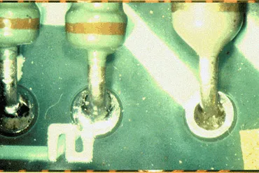
- Pad Size and Shape: Use pads that are slightly larger than the component lead diameter to allow for proper solder flow. A general rule is to make the pad diameter 1.5 to 2 times the lead diameter. For example, if a component lead is 0.8 mm in diameter, the pad should be 1.2 to 1.6 mm in diameter. Oval or teardrop-shaped pads can improve solder flow and reduce the risk of defects.
- Annular Ring: Ensure a sufficient annular ring (the copper area surrounding the drilled hole) to provide structural integrity. A minimum annular ring of 0.25 mm (10 mils) on each side of the hole is a common standard for through-hole pads.
- Thermal Relief Pads: For components connected to large copper planes (like ground or power planes), use thermal relief pads. These pads have small connecting traces (spokes) to the plane, which prevent excessive heat dissipation during soldering. This ensures the solder joint reaches the necessary temperature. A typical thermal relief design includes four spokes, each 0.2 to 0.3 mm wide.
- Drill Hole Size: The drilled hole for through-hole leads should be slightly larger than the lead diameter to allow easy insertion and solder flow. A hole diameter of lead size plus 0.1 to 0.2 mm is often ideal. For instance, a 0.8 mm lead should have a hole size of 0.9 to 1.0 mm.
3. Wave Soldering Thermal Considerations
Thermal management is essential during wave soldering to prevent component damage and ensure consistent solder joints. Here are key wave soldering thermal considerations for your PCB design:
- Minimize Large Copper Areas Near Components: Large copper planes can act as heat sinks, drawing heat away from pads and preventing proper solder joint formation. As mentioned earlier, use thermal relief pads to isolate component pads from large copper areas.
- Balance Copper Distribution: Uneven copper distribution across the PCB can lead to thermal imbalances, causing the board to warp or develop hot spots during soldering. Distribute copper evenly on both sides of the board to maintain uniform heat distribution.
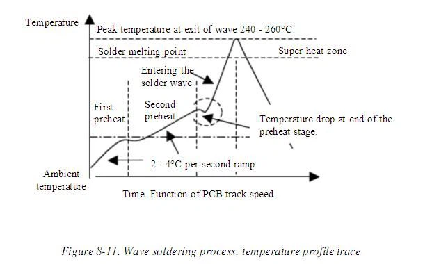
- Component Thermal Sensitivity: Some components, like certain capacitors or ICs, are sensitive to high temperatures. Check the datasheet for maximum temperature ratings and ensure the wave soldering profile (temperature and duration) stays within safe limits. For example, many components can withstand 260°C for 10 seconds, which aligns with typical wave soldering conditions.
- Preheat Stage: Wave soldering machines often include a preheat stage to gradually raise the PCB temperature before it contacts the solder wave. This reduces thermal shock to components and the board. Ensure your design allows for even preheating by avoiding overly dense component clusters.
4. Board Layout and Solder Mask Considerations
The overall board layout and solder mask design also play a role in successful wave soldering. Keep these points in mind:
- Solder Mask Clearance: Provide adequate clearance between the solder mask and pads to prevent mask overlap, which can interfere with solder flow. A clearance of 0.1 to 0.2 mm around pads is typically sufficient.
- Fiducial Marks: Include fiducial marks on the PCB for alignment during automated assembly and soldering. Place at least two fiducials diagonally across the board for accurate positioning.
- Board Edge Clearance: Leave a margin of at least 5 mm around the PCB edges free of components. This allows for proper handling and conveyor alignment during wave soldering.
Common Wave Soldering Defects and How to Avoid Them
Even with a well-designed PCB, wave soldering can result in defects if certain pitfalls aren’t addressed. Here are common issues and how to prevent them through design:
- Solder Bridging: This occurs when solder connects adjacent pads or leads. Prevent it by maintaining proper spacing (at least 2.54 mm between leads) and aligning components with the wave direction.
- Insufficient Solder: If pads don’t receive enough solder, joints may be weak. Ensure pad sizes are adequate (1.5 to 2 times the lead diameter) and avoid shadowing by placing taller components at the trailing edge of the wave.
- Cold Solder Joints: These weak joints form when pads don’t reach the required temperature. Use thermal relief pads and balance copper distribution to ensure even heating.
- Component Damage: Excessive heat can damage sensitive components. Verify that the wave soldering temperature profile matches the thermal limits specified in component datasheets.
Testing and Validation After Wave Soldering
Once your PCB has been wave soldered, it’s important to validate the quality of the assembly. Here are steps to ensure your design and soldering process were successful:
- Visual Inspection: Check for visible defects like solder bridging, cold joints, or misaligned components. Use a magnifying glass or microscope for detailed examination of solder joints.
- Electrical Testing: Perform continuity and functional tests to confirm that all connections are intact and the circuit operates as intended.
- Thermal Stress Testing: Subject the PCB to temperature cycling to verify that solder joints can withstand thermal expansion and contraction without cracking.
Conclusion: Optimize Your PCB Design for Wave Soldering Success
Designing a PCB for wave soldering requires careful attention to component placement, pad design, and thermal management. By following wave soldering PCB design rules—such as aligning components with the solder wave, using appropriately sized pads with thermal relief, and balancing copper distribution—you can minimize defects and achieve reliable solder joints. Additionally, considering wave soldering component orientation, pad design for through-hole parts, and thermal considerations ensures your board withstands the soldering process without damage.
Implementing these best practices not only improves manufacturing yields but also enhances the long-term reliability of your electronic products. Take the time to review your design against these guidelines, and you’ll be well on your way to creating high-quality PCBs optimized for wave soldering.


