ALLPCB


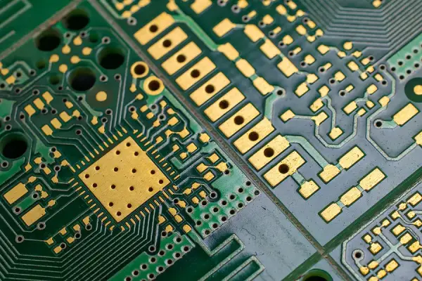
If you're in the world of printed circuit boards (PCBs), you may have come across the term "black pad" in relation to ENIG (Electroless Nickel Immersion Gold) surface finishes. So, what does black pad mean? In simple terms, black pad refers to a defect in the ENIG finish where the nickel layer corrodes, leading to poor solderability and potential failure of the PCB. This issue can severely impact the reliability of electronic devices, making it a critical concern for engineers and manufacturers.
In this detailed guide, we'll dive deep into the concept of black pad, explore its causes, effects, and prevention methods, and provide actionable insights for those dealing with PCB manufacturing. Whether you're a design engineer or a quality control specialist, understanding black pad ENIG defects on PCBs is essential for ensuring high-quality, reliable products. Let's break it down step by step.
Understanding Black Pad in PCB Manufacturing
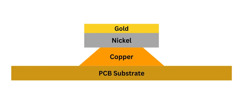
Black pad is a specific defect associated with the ENIG surface finish, a popular choice for PCBs due to its excellent solderability and corrosion resistance. ENIG involves depositing a layer of nickel onto the copper pads of a PCB, followed by a thin layer of gold to protect the nickel from oxidation. However, under certain conditions, the nickel layer can corrode during the gold deposition process, forming a black or dark layer of nickel oxide or other compounds. This corroded layer is what we refer to as "black pad."
This defect isn't just a cosmetic issue. The presence of black pad can weaken the bond between the solder and the pad, leading to brittle solder joints that may crack or fail during assembly or operation. For industries where reliability is non-negotiable—such as aerospace, medical, and automotive—black pad defects on PCBs can have catastrophic consequences.
Why Is It Called Black Pad?
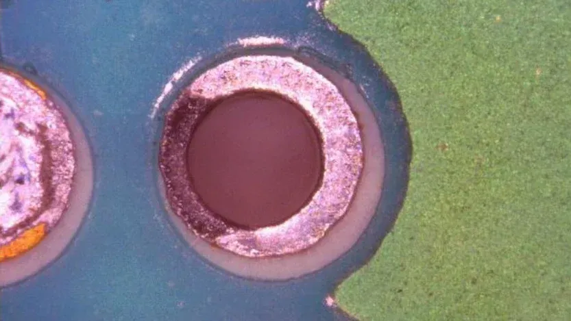
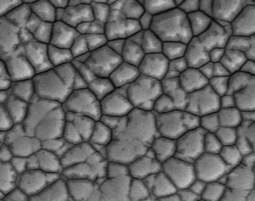
The term "black pad" comes from the visual appearance of the defect. When the nickel layer corrodes, it often turns dark or black due to the formation of nickel oxides or other compounds. Under a microscope, these affected areas may show cracks, uneven surfaces, or a grainy texture, making them stand out from the smooth, shiny finish of unaffected pads.
Causes of Black Pad ENIG Defects on PCBs
To tackle black pad issues, it's crucial to understand what causes this defect in the first place. Several factors during the ENIG plating process can contribute to the formation of black pad. Below are the primary causes:
- High Phosphorus Content in Nickel Layer: During the electroless nickel plating process, phosphorus is often incorporated into the nickel layer to enhance corrosion resistance. However, if the phosphorus content is too high (typically above 10-12% by weight), it can lead to the formation of a phosphorus-rich layer that corrodes easily during gold immersion, resulting in black pad.
- Improper Gold Immersion Process: The immersion gold step involves a chemical reaction where nickel is displaced by gold. If the process is not tightly controlled—such as with incorrect pH levels, temperature, or immersion time—excessive nickel corrosion can occur, forming black pad.
- Contamination in Plating Solutions: Contaminants in the nickel or gold plating baths, such as organic residues or metallic impurities, can interfere with the plating process, leading to uneven deposition and corrosion of the nickel layer.
- Poor Process Control: Inconsistent monitoring of plating parameters like temperature, agitation, or bath composition can result in defects. For instance, a bath temperature outside the optimal range of 80-90°C during nickel plating can affect the layer's integrity.
- Extended Metal Turnover (MTO): As plating baths are reused, the accumulation of byproducts and dissolved metals (measured as metal turnover or MTO) can degrade bath quality, increasing the likelihood of black pad formation.
Understanding these root causes is the first step toward preventing black pad ENIG defects on PCBs. Each of these factors highlights the importance of precision and quality control in the manufacturing process.
Effects of Black Pad on PCB Reliability
Black pad might seem like a minor issue at first glance, but its impact on PCB performance and reliability can be significant. Here’s how this defect affects the final product:
- Poor Solderability: The corroded nickel layer prevents proper wetting of solder, leading to weak or incomplete solder joints. This can cause components to detach during assembly or fail under thermal or mechanical stress.
- Brittle Solder Joints: Even if solder adheres to the pad, the presence of black pad can create a brittle intermetallic compound (IMC) layer. Studies have shown that these joints can fail at stress levels as low as 10-15 MPa, compared to over 30 MPa for defect-free joints.
- Reduced Product Lifespan: Black pad defects often lead to premature failure of electronic devices, especially in harsh environments where temperature cycling (e.g., -40°C to 85°C) or vibration is common.
- Increased Manufacturing Costs: Detecting and addressing black pad issues often requires additional testing, rework, or scrapping of defective boards, driving up production costs.
For engineers designing high-reliability systems, black pad is a defect that must be addressed proactively to avoid costly failures in the field.
How to Detect Black Pad Defects on PCBs
Detecting black pad can be challenging because it’s not always visible to the naked eye during early stages. However, several inspection methods can help identify this defect before it causes problems:
- Visual Inspection Under Magnification: Using a microscope with 10x to 50x magnification, inspectors can look for dark or discolored areas on the pads, as well as cracks or uneven surfaces.
- Solderability Testing: Performing a solderability test, such as the dip-and-look method, can reveal whether solder wets the pad properly. Poor wetting or dewetting indicates a potential black pad issue.
- Cross-Sectional Analysis: Cutting a sample of the PCB and examining the pad’s cross-section under a scanning electron microscope (SEM) can show the thickness and condition of the nickel and gold layers. A corroded nickel layer often appears as a dark band.
- Energy Dispersive X-Ray Spectroscopy (EDS): This technique analyzes the chemical composition of the pad surface, detecting high levels of phosphorus or oxygen that indicate corrosion.
Early detection through these methods can save significant time and resources by preventing defective boards from reaching assembly or end users.
Preventing Black Pad ENIG Defects on PCBs
Prevention is always better than cure, especially when it comes to black pad defects. By optimizing the manufacturing process and adhering to strict quality controls, manufacturers can significantly reduce the risk of black pad. Here are some effective strategies:
- Control Phosphorus Levels: Maintain phosphorus content in the nickel layer within the recommended range of 7-9% by weight. Regular analysis of the plating bath can help ensure consistency.
- Optimize Gold Immersion Parameters: Keep immersion gold process parameters—such as pH (typically 4.5-5.5), temperature (80-85°C), and time (10-15 minutes)—within specified limits to minimize nickel corrosion.
- Use High-Quality Plating Solutions: Regularly filter and replenish plating baths to remove contaminants. Monitor metal turnover and replace baths after a specific number of cycles, often around 5-6 MTO, depending on the formulation.
- Implement Process Monitoring: Use real-time monitoring tools to track bath temperature, agitation, and chemical composition. Automated systems can alert operators to deviations before they cause defects.
- Adhere to IPC Standards: Follow guidelines from the Institute of Printed Circuits (IPC), such as IPC-4552, which specifies requirements for ENIG finishes, including nickel thickness (3-6 μm) and gold thickness (0.05-0.1 μm), to ensure reliability.
- Conduct Regular Testing: Perform routine solderability and adhesion tests on sample boards to catch potential black pad issues early in the production process.
By integrating these practices into the manufacturing workflow, the likelihood of black pad ENIG defects on PCBs can be minimized, ensuring higher quality and reliability.
Solutions for Addressing Black Pad Issues
If black pad defects are detected after manufacturing, there are a few approaches to mitigate the issue, though prevention remains the best strategy. Here are some solutions:
- Reworking Affected Boards: In some cases, affected pads can be cleaned or re-plated with a new ENIG layer. However, this is often costly and may not guarantee long-term reliability.
- Switching to Alternative Finishes: If black pad issues persist, consider using alternative surface finishes like Immersion Silver or OSP (Organic Solderability Preservative), which do not involve nickel plating and thus avoid black pad risks. However, each finish has its own trade-offs in terms of cost and performance.
- Enhanced Quality Assurance: Implement stricter incoming material inspections and supplier audits to ensure that raw materials and plating chemicals meet required standards.
While these solutions can help manage black pad defects, they often come with additional costs or complexity. Focusing on prevention during the initial manufacturing stages is usually the most effective approach.
Why Choose a Reliable PCB Manufacturing Partner?
Navigating the complexities of black pad and other ENIG defects requires expertise, advanced equipment, and stringent quality control processes. Partnering with a trusted PCB manufacturing service can make all the difference in achieving defect-free boards. A reliable manufacturer will have robust systems in place to monitor plating processes, adhere to industry standards, and conduct thorough testing to ensure the highest quality.
At ALLPCB, we prioritize precision and reliability in every step of the PCB production process. Our state-of-the-art facilities and experienced team are equipped to handle the challenges of ENIG finishes, helping you avoid issues like black pad and deliver top-notch products to your customers.
Conclusion
Black pad is a critical defect in the ENIG surface finish of PCBs, caused by nickel corrosion during the plating process. This issue, often linked to high phosphorus content, improper process control, or contamination, can lead to poor solderability, brittle joints, and reduced product reliability. By understanding the causes and effects of black pad ENIG defects on PCBs, engineers and manufacturers can take proactive steps to detect and prevent this issue through optimized processes, regular testing, and adherence to industry standards.
With the right knowledge and manufacturing practices, black pad doesn’t have to be a persistent problem. By focusing on quality control and partnering with experienced PCB providers, you can ensure that your boards meet the highest standards of performance and durability. Stay informed, stay vigilant, and keep your designs free from the risks of black pad defects.