ALLPCB


In the world of electronics manufacturing, ensuring the quality and reliability of printed circuit boards (PCBs) is critical. Hidden defects, such as internal cracks, voids, or poor solder joints, can lead to catastrophic failures if not detected early. So, how do manufacturers uncover these invisible flaws without damaging the board? The answer lies in X-ray PCB inspection, a powerful non-destructive testing method. This blog explores the intricacies of PCB internal defect detection, the non-destructive PCB testing process, and a detailed look at the X-ray inspection process, helping engineers and manufacturers ensure top-notch quality in their products.
Why PCB Internal Defect Detection Matters
PCBs are the backbone of modern electronics, from smartphones to medical devices. As designs become more complex with multi-layer boards and miniaturized components, the risk of internal defects increases. These defects, often hidden beneath layers of material, can include issues like delamination, insufficient solder, or misaligned vias. If left undetected, they can cause short circuits, signal loss, or complete device failure.
Traditional visual inspection methods fall short when it comes to identifying internal issues. This is where non-destructive PCB testing, particularly X-ray inspection, becomes indispensable. By allowing manufacturers to see inside the board without breaking it apart, X-ray technology ensures that even the smallest flaws are caught before they become bigger problems.
What Is X-Ray PCB Inspection?
X-ray PCB inspection is a non-destructive testing technique that uses X-ray radiation to penetrate the layers of a printed circuit board and create detailed images of its internal structure. Unlike optical inspections that rely on surface-level analysis, X-ray systems can reveal hidden defects within solder joints, vias, and component connections. This method is especially crucial for modern PCBs with dense layouts and surface-mount components that are difficult to inspect manually.
The process involves passing X-rays through the PCB, where denser materials like metal absorb more radiation and appear darker on the resulting image, while less dense areas appear lighter. This contrast helps engineers identify anomalies such as voids in solder joints or misaligned components with precision.
The Importance of Non-Destructive PCB Testing
Non-destructive testing (NDT) methods, like X-ray inspection, are vital in electronics manufacturing because they allow for thorough quality checks without damaging the product. Destructive testing, such as cutting open a PCB for analysis, not only ruins the sample but also fails to provide a scalable solution for mass production. Non-destructive PCB testing, on the other hand, ensures that every board can be inspected and still used in the final product if it passes the quality standards.
X-ray inspection stands out among NDT methods due to its ability to detect internal defects that other techniques, like automated optical inspection (AOI), cannot. For instance, AOI systems use light to inspect surface features but cannot penetrate the board to check for hidden issues. X-ray technology fills this gap, making it an essential tool for ensuring reliability in high-stakes applications like aerospace or medical electronics.
How the X-Ray Inspection Process Works
The X-ray inspection process for PCBs is a systematic approach that involves several key steps. Understanding this process can help manufacturers integrate it effectively into their quality control workflows. Below is a detailed breakdown of how it works:
1. Preparation of the PCB
Before inspection begins, the PCB is prepared by ensuring it is clean and free from contaminants that could interfere with the imaging process. The board is then placed on a specialized tray or fixture inside the X-ray machine to hold it steady during scanning. Proper positioning is crucial to obtain clear and accurate images of the internal structures.
2. X-Ray Emission and Penetration
Once the PCB is in place, the X-ray machine emits controlled radiation that passes through the board. The system typically uses a low-energy X-ray source to avoid damaging the components while still providing sufficient penetration. As the X-rays travel through the PCB, they interact differently with materials of varying densities. For example, copper traces and solder joints absorb more radiation and appear darker, while insulating materials like fiberglass appear lighter.
3. Image Capture and Processing
A detector on the opposite side of the PCB captures the X-rays that pass through, converting them into a digital image. Advanced software processes these images to enhance clarity and highlight potential defects. Some systems offer 2D imaging for basic inspections, while others provide 3D computed tomography (CT) for a more detailed view of complex multi-layer boards.
4. Defect Analysis
Engineers or automated algorithms analyze the captured images to identify defects. Common issues detected include voids in solder joints (often as small as 0.1 mm in diameter), misaligned components, or cracks in internal layers. The software can quantify defect sizes and locations, providing precise data for decision-making.
5. Reporting and Decision-Making
After analysis, a detailed report is generated, documenting any defects found and their severity. Based on this information, manufacturers decide whether the PCB meets quality standards or requires rework. This step ensures that only reliable boards move forward in the production process.
Common Internal Defects Detected by X-Ray Inspection
X-ray PCB inspection excels at uncovering a wide range of internal defects that could compromise the performance of a board. Here are some of the most common issues it can detect:
- Voids in Solder Joints: Small air pockets or gaps in solder can weaken connections and lead to failures. X-ray systems can detect voids as small as 5-10% of the joint volume, ensuring robust connections.
- Insufficient Solder: Areas with too little solder may not provide a stable electrical connection, increasing resistance and heat buildup. X-ray images reveal these thin spots clearly.
- Bridging or Shorts: Unintended connections between solder points can cause short circuits. X-ray inspection identifies these issues even when hidden under components.
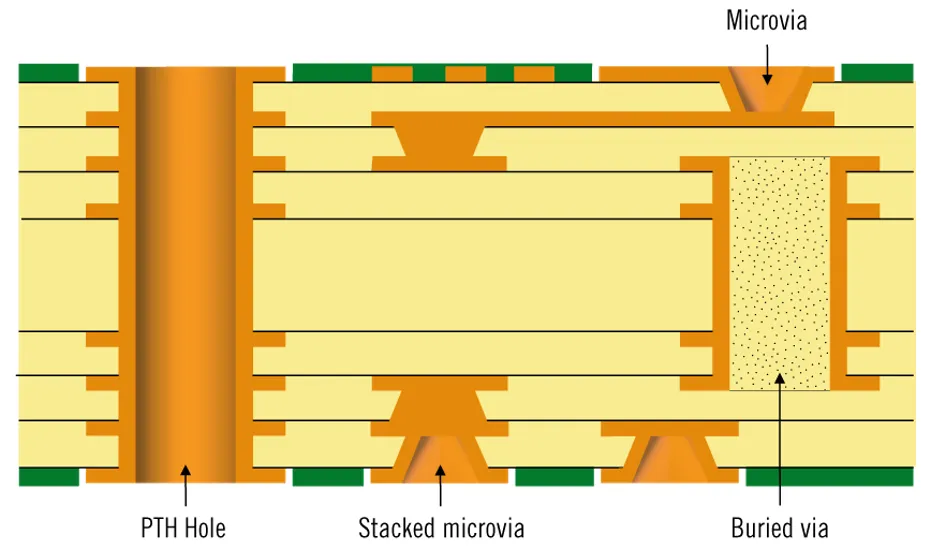
- Delamination: Separation of layers within a multi-layer PCB can disrupt signal integrity. X-ray imaging shows these internal gaps that are invisible to the naked eye.
- Misaligned Components or Vias: Tiny misalignments in component placement or via drilling can affect performance. X-ray systems provide precise measurements to confirm alignment within tolerances as tight as 0.05 mm.
By catching these defects early, manufacturers can prevent costly recalls and ensure the reliability of their products in demanding applications.
Benefits of X-Ray PCB Inspection for Manufacturers
Integrating X-ray inspection into the PCB manufacturing process offers numerous advantages, especially as electronics continue to shrink in size and grow in complexity. Here are some key benefits:
Enhanced Quality Control
X-ray inspection provides a level of detail that other testing methods cannot match. It ensures that every board meets strict quality standards, reducing the risk of field failures. For example, in high-reliability sectors like automotive electronics, where failure rates must be below 1 part per million (PPM), X-ray testing is often a mandatory step.
Cost Savings in the Long Run
While X-ray equipment requires an initial investment, it saves money by preventing defective boards from reaching customers. Detecting a fault during production is far less expensive than handling warranty claims or recalls. Studies suggest that early defect detection can reduce overall quality-related costs by up to 30%.
Support for Complex Designs
As PCBs incorporate more layers (sometimes exceeding 20 layers) and smaller components (like 0201-sized resistors), traditional inspection methods struggle to keep up. X-ray systems can handle these challenges, providing clear images of dense layouts and fine-pitch connections.
Non-Destructive Nature
Unlike destructive testing, X-ray inspection preserves the integrity of the PCB. This means manufacturers can test 100% of their boards if needed, without sacrificing any product, which is especially valuable for small-batch or high-value production runs.
Challenges and Considerations in X-Ray PCB Inspection
While X-ray inspection is a powerful tool, it’s not without its challenges. Manufacturers must consider several factors to ensure effective implementation:
- Equipment Cost: High-quality X-ray systems can be expensive, with prices ranging from tens of thousands to hundreds of thousands of dollars. However, the return on investment often justifies the cost for large-scale or high-reliability production.
- Operator Training: Interpreting X-ray images requires skilled personnel or advanced software. Misreading an image could lead to false positives or missed defects, so proper training is essential.
- Radiation Safety: Although modern X-ray machines use low-energy radiation and are designed with safety in mind, strict protocols must be followed to protect operators from exposure.
- Inspection Speed: While automated X-ray systems are faster than manual methods, they can still be slower than other techniques like AOI for surface defects. Balancing speed and thoroughness is key.
By addressing these challenges, manufacturers can maximize the effectiveness of X-ray inspection and integrate it seamlessly into their quality assurance processes.
Applications of X-Ray Inspection Across Industries
X-ray PCB inspection is widely used across various industries where reliability and precision are non-negotiable. Here are a few examples:
- Aerospace: PCBs in satellites and aircraft must withstand extreme conditions. X-ray testing ensures that internal connections are flawless to prevent failures in critical systems.
- Medical Devices: From pacemakers to imaging equipment, medical electronics require zero defects. X-ray inspection verifies the integrity of every component and connection.
- Automotive: With the rise of electric vehicles and advanced driver-assistance systems (ADAS), automotive PCBs must handle high currents and complex signals. X-ray systems detect flaws that could lead to safety hazards.
- Consumer Electronics: As devices like smartphones become smaller and more powerful, X-ray inspection ensures that densely packed boards meet quality standards.
These applications highlight the versatility and necessity of X-ray PCB inspection in today’s technology-driven world.
Future Trends in X-Ray PCB Inspection
As technology evolves, so does the field of X-ray PCB inspection. Several trends are shaping the future of this critical testing method:
- Advancements in 3D Imaging: 3D X-ray computed tomography (CT) is becoming more accessible, allowing for detailed cross-sectional views of multi-layer PCBs. This technology can detect defects with even greater accuracy, down to sub-micron levels.
- Artificial Intelligence Integration: AI-powered software is being developed to automate defect detection and classification in X-ray images. This reduces human error and speeds up the inspection process, with some systems achieving analysis times of under 10 seconds per board.
- Miniaturization of Equipment: Newer X-ray systems are becoming more compact and affordable, making them accessible to smaller manufacturers without sacrificing performance.
- Higher Resolution Capabilities: Improvements in detector technology are enabling higher resolution images, allowing for the detection of defects in even the smallest components, such as 01005-sized chips.
These innovations promise to make X-ray PCB inspection even more effective and widely adopted in the coming years.
Conclusion: Ensuring Reliability with X-Ray PCB Inspection
In the fast-paced world of electronics manufacturing, ensuring the quality of printed circuit boards is more important than ever. Hidden defects can lead to costly failures, but with X-ray PCB inspection, manufacturers can uncover these issues without damaging the product. This non-destructive PCB testing method offers unparalleled insight into internal structures, making it an essential tool for PCB internal defect detection.
By understanding the X-ray inspection process and its benefits, engineers and manufacturers can implement robust quality control measures that meet the demands of modern electronics. From detecting tiny voids in solder joints to verifying the alignment of complex multi-layer boards, X-ray technology is a game-changer in ensuring reliability and performance. As advancements continue to emerge, this method will only become more vital in delivering flawless products to the market.