 ALLPCB


In the fast-evolving world of telecommunications, 5G technology stands as a game-changer, promising blazing-fast speeds, ultra-low latency, and massive connectivity. But what makes 5G truly work at its peak? The answer lies in the heart of the devices and infrastructure: high-frequency printed circuit boards (PCBs). If you're looking to understand 5G PCB materials, high-frequency PCB design for 5G, mmWave PCB manufacturing, 5G antenna PCB, or low-loss PCB for 5G, you're in the right place. This blog will explore how advanced PCB manufacturing unlocks the full potential of 5G technology, diving deep into materials, design techniques, and manufacturing challenges.
At its core, 5G performance depends on PCBs that can handle extremely high frequencies, especially in the millimeter-wave (mmWave) spectrum, while minimizing signal loss. Let’s break down the critical aspects of high-frequency PCB manufacturing to help engineers and tech enthusiasts navigate this cutting-edge field with actionable insights.
Why High-Frequency PCBs Are Critical for 5G Technology
5G networks operate at much higher frequencies than 4G, ranging from sub-6 GHz to mmWave bands as high as 24-100 GHz. These frequencies enable data speeds up to 100 times faster than 4G and latency below 1 millisecond. However, they also pose unique challenges for PCB design and manufacturing. High-frequency signals are more sensitive to interference, signal loss, and material properties, making the choice of materials and design techniques vital.
Traditional PCBs, often made with standard materials like FR4, struggle to maintain signal integrity at these frequencies due to higher dielectric losses and poor thermal management. This is where high-frequency PCBs come in, tailored to support 5G's demanding requirements, from base stations to IoT devices and 5G-enabled smartphones.
Key Challenges in High-Frequency PCB Design for 5G
Designing PCBs for 5G is no easy task. Engineers must overcome several hurdles to ensure performance and reliability. Here are the primary challenges:
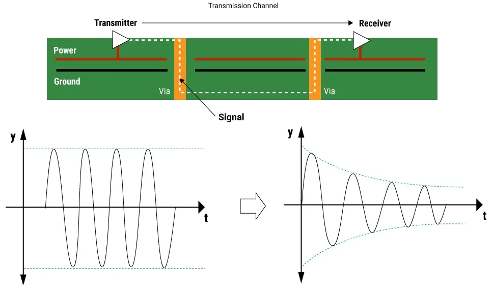
- Signal Integrity at High Frequencies: At mmWave frequencies, even small imperfections in the PCB can cause significant signal degradation. For instance, a via (a small hole connecting layers) can introduce a loss of 0.1-0.2 dB at 10 GHz. Designers must minimize via usage in critical signal paths.
- Thermal Management: High-frequency circuits generate more heat, especially in compact 5G devices. Poor heat dissipation can affect performance and longevity.
- Material Limitations: Standard materials often fail at frequencies above 1 GHz due to high dielectric loss, making specialized laminates a necessity.
- Manufacturing Precision: The tight tolerances required for mmWave PCB manufacturing demand advanced fabrication techniques to avoid errors in trace width or spacing, which can disrupt impedance control.
Addressing these challenges starts with selecting the right materials and optimizing the design for high-frequency performance.
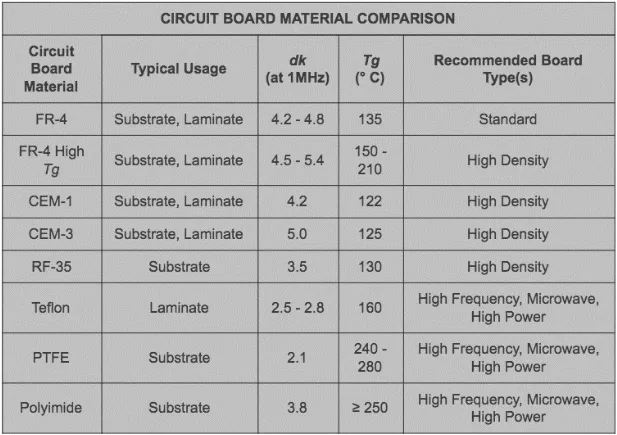
Choosing the Right 5G PCB Materials for Optimal Performance
The foundation of any high-frequency PCB lies in its material. For 5G applications, the material must have a low dielectric constant (Dk) and low dissipation factor (Df) to reduce signal loss. Here are some key considerations for selecting 5G PCB materials:
- Low-Loss Laminates: Materials with low Df values (below 0.003 at 10 GHz) are ideal for minimizing signal attenuation in low-loss PCB for 5G designs. Popular options include PTFE-based laminates and hydrocarbon ceramic composites, which offer excellent performance in mmWave bands.
- Dielectric Constant Stability: A stable Dk across a wide frequency range ensures consistent signal speed and impedance. For example, a Dk variation of just 0.1 can cause phase shifts in high-frequency signals.
- Thermal Conductivity: Materials with high thermal conductivity help dissipate heat in densely packed 5G circuits, ensuring reliability.
Unlike traditional FR4, which is cost-effective but unsuitable for frequencies above 1 GHz, advanced materials are specifically engineered for 5G. These materials are widely used in 5G antenna PCB designs and base station equipment, where signal clarity is non-negotiable.
High-Frequency PCB Design Techniques for 5G
Once the material is chosen, the next step is optimizing the high-frequency PCB design for 5G. Here are some proven techniques to ensure performance:
1. Controlled Impedance Design
Impedance matching is critical at high frequencies to prevent signal reflection. For 5G circuits operating at mmWave frequencies, designers often target a characteristic impedance of 50 ohms for transmission lines. Even a 5% mismatch can lead to significant signal loss.
2. Minimizing Signal Path Lengths
Shorter signal paths reduce the chance of loss and interference. In mmWave PCB manufacturing, designers route critical signals on the top layer whenever possible to avoid vias and cross-talk.
3. Ground Plane Optimization
A solid ground plane beneath high-frequency traces helps reduce electromagnetic interference (EMI). Stitching vias around the ground plane can further enhance shielding, especially in compact 5G devices.
4. Skin Effect Consideration
At high frequencies, the skin effect causes current to flow primarily on the surface of conductors. Rough copper surfaces increase resistance and loss, so smooth copper foils are preferred in 5G designs to maintain signal integrity.
By implementing these techniques, engineers can build PCBs that meet the stringent demands of 5G applications, from consumer gadgets to industrial IoT systems.
The Role of 5G Antenna PCB in Network Performance
Antennas are the gateway for 5G signals, and their performance heavily depends on the underlying PCB. A well-designed 5G antenna PCB ensures efficient signal transmission and reception, especially in the mmWave spectrum where beamforming is used to focus signals.
Key factors in 5G antenna PCB design include:
- Array Integration: 5G often uses phased array antennas with multiple elements to enable beamforming. The PCB must support precise spacing and alignment of these elements, often within tolerances of 0.1 mm.
- Material Selection: Low-loss materials are critical to prevent energy loss in the antenna structure, ensuring maximum range and efficiency.
- Compact Layouts: With 5G devices becoming smaller, antenna PCBs must fit into tight spaces without sacrificing performance.
Advanced manufacturing processes are essential to achieve the precision required for these designs, especially for applications like autonomous vehicles and smart cities.
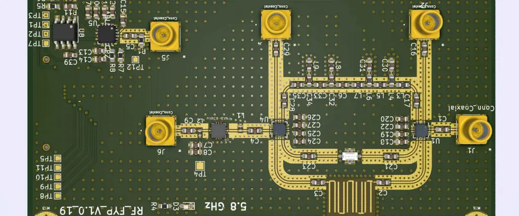
mmWave PCB Manufacturing: Precision at Its Core
mmWave PCB manufacturing is a specialized field that pushes the boundaries of fabrication technology. Operating at frequencies above 24 GHz, mmWave PCBs require exceptional precision and quality control. Here’s what sets this process apart:
- Tight Tolerances: Trace widths and spacing often need to be controlled within ±0.001 inches to maintain impedance and prevent signal distortion.
- Advanced Layering: Multilayer designs are common in mmWave PCBs to accommodate complex circuits. However, each additional layer increases the risk of misalignment, demanding high-end manufacturing equipment.
- Surface Finish: Smooth surface finishes, such as ENIG (Electroless Nickel Immersion Gold), are preferred to reduce signal loss caused by surface roughness.
The manufacturing process for mmWave PCBs also involves rigorous testing to ensure performance. For instance, network analyzers are used to measure signal loss and impedance across the frequency range, ensuring the board meets 5G standards.
Low-Loss PCB for 5G: Maximizing Efficiency
Signal loss is the enemy of 5G performance, and low-loss PCB for 5G designs are the solution. These boards are engineered to minimize attenuation, ensuring that high-frequency signals travel with minimal degradation. Here’s how low-loss PCBs make a difference:
- Reduced Dielectric Loss: Using materials with a low dissipation factor ensures that less signal energy is absorbed by the substrate. For example, a Df of 0.002 can reduce loss by up to 20% compared to standard materials at 28 GHz.
- Optimized Trace Geometry: Wider traces and shorter lengths help lower resistance and maintain signal strength.
- Shielding Techniques: Proper shielding reduces cross-talk and external interference, preserving signal quality.
Low-loss PCBs are particularly important in applications like 5G base stations, where long-distance signal transmission must remain clear and reliable.
Future Trends in 5G PCB Manufacturing
As 5G adoption grows, so does the demand for innovative PCB solutions. Industry forecasts suggest that by 2032, the market for high-frequency materials will reach $3.8 billion, driven by the expansion of 5G networks. Here are some trends to watch:
- Hybrid Materials: Combining different substrates in a single PCB to balance cost and performance for specific frequency bands.
- Miniaturization: Smaller, denser PCBs to support compact 5G devices without compromising signal quality.
- Sustainable Manufacturing: A push toward eco-friendly materials and processes to reduce the environmental impact of PCB production.
Staying ahead of these trends ensures that manufacturers and engineers can meet the evolving needs of 5G technology.
How ALLPCB Supports 5G PCB Manufacturing
Navigating the complexities of high-frequency PCB manufacturing for 5G requires a trusted partner with expertise and cutting-edge capabilities. At ALLPCB, we specialize in delivering tailored solutions for 5G applications, from material selection to precision fabrication. Our advanced manufacturing processes ensure tight tolerances, low signal loss, and reliable performance for everything from antenna designs to base station components.
Whether you’re working on mmWave PCB manufacturing or need a low-loss PCB for 5G, our team is ready to support your project with professional guidance and high-quality results. With a focus on innovation, we help engineers unlock the full potential of 5G technology through optimized PCB solutions.
Conclusion: Powering the Future with High-Frequency PCBs
The rise of 5G technology is reshaping the world of connectivity, and high-frequency PCBs are at the forefront of this revolution. By understanding the importance of 5G PCB materials, mastering high-frequency PCB design for 5G, and leveraging advanced mmWave PCB manufacturing techniques, engineers can build the infrastructure and devices that power tomorrow’s networks.
From 5G antenna PCB designs to low-loss PCB for 5G applications, every aspect of PCB manufacturing plays a vital role in achieving peak performance. As the demand for faster, more reliable connectivity grows, staying informed about materials, design strategies, and manufacturing innovations will be key to success in this dynamic field.
At ALLPCB, we’re committed to helping you navigate these challenges and bring your 5G projects to life. Let’s build the future of connectivity together with precision-engineered PCBs designed for the next generation of technology.


