 ALLPCB


If you're designing a printed circuit board (PCB), one of the most critical aspects to get right is trace spacing. But what exactly is minimum trace spacing, and how does it vary between different PCB layers like inner and outer layers? In simple terms, minimum trace spacing is the smallest distance allowed between two conductive traces on a PCB to ensure safety, signal integrity, and manufacturability. This spacing differs based on whether you're working on inner layers (sandwiched inside the board) or outer layers (exposed on the top and bottom), as well as factors like voltage, manufacturing capabilities, and design standards. In this blog, we'll dive deep into trace spacing for PCB layers, focusing on inner and outer layer design, and provide practical insights for your next project.
What Is Trace Spacing in PCB Design?
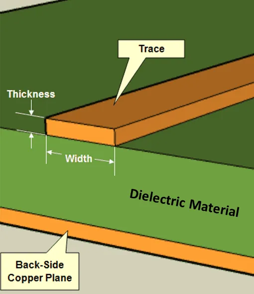
Trace spacing refers to the distance between adjacent conductive paths, or traces, on a PCB. These traces carry electrical signals or power between components, and maintaining the right spacing is crucial to prevent issues like electrical shorts, crosstalk, or signal interference. The minimum trace spacing is determined by several factors, including the voltage levels of the signals, the type of PCB material, and the manufacturing process.
In PCB manufacturing, trace spacing is not a one-size-fits-all value. It varies depending on whether the traces are on the outer layers (the top and bottom surfaces of the board) or the inner layers (the layers stacked inside a multilayer PCB). Understanding these differences is key to designing a board that performs reliably and can be manufactured without issues.
Why Minimum Trace Spacing Matters
Getting trace spacing right is essential for several reasons. First, it ensures electrical safety by preventing arcing or short circuits between traces, especially in high-voltage designs. Second, it helps maintain signal integrity by reducing crosstalk and electromagnetic interference (EMI) between adjacent traces. Lastly, it ensures that your design is manufacturable—too tight spacing can lead to production errors or defects during etching and fabrication.
For engineers and designers, adhering to minimum trace spacing guidelines is not just about meeting standards; it's about ensuring the reliability and performance of the final product. Let's break down how these requirements differ for inner and outer layers in PCB design.
Trace Spacing for Outer Layers
Outer layers are the top and bottom surfaces of a PCB, directly exposed to the environment or covered by a solder mask. Because of this exposure, trace spacing on outer layers often has specific constraints influenced by manufacturing processes and environmental factors.
Typically, the minimum trace spacing on outer layers is slightly more forgiving than on inner layers due to the ease of etching and inspection. For standard designs with voltages below 50V, a common minimum spacing might be around 6 mils (0.006 inches or 0.152 mm). However, this value increases with higher voltages to prevent arcing. For example, at 100V, you might need a spacing of at least 12 mils (0.012 inches or 0.305 mm), based on industry standards like IPC-2221, which provides guidelines for PCB design.
Outer layer spacing is also influenced by the solder mask. While the solder mask adds a layer of insulation, it’s not considered a reliable barrier for high-voltage applications. Therefore, designers must still adhere to spacing rules as if the mask wasn’t there, especially for safety-critical designs.
Factors Affecting Outer Layer Spacing
- Voltage Levels: Higher voltages require larger spacing to prevent electrical breakdown or arcing. For instance, a design operating at 500V may need spacing of up to 50 mils (0.05 inches or 1.27 mm).
- Environmental Conditions: Outer layers are more exposed to humidity, dust, and contaminants, which can reduce insulation effectiveness. Designers may need to increase spacing in harsh environments.
- Manufacturing Tolerances: The etching process for outer layers can vary, so it’s important to design with a buffer above the absolute minimum spacing to account for potential inconsistencies.
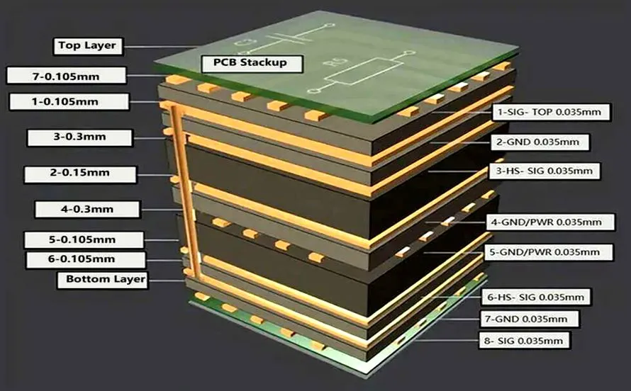
Trace Spacing for Inner Layers
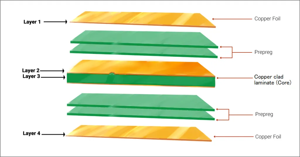
Inner layers are the copper layers sandwiched between insulating materials (like prepreg) in a multilayer PCB. These layers are not exposed to the environment, which might suggest that spacing could be tighter. However, inner layer trace spacing often has stricter requirements due to other factors like heat dissipation and signal integrity.
For inner layers, minimum trace spacing is often similar to or slightly tighter than outer layers for low-voltage designs, typically starting at 5-6 mils (0.005-0.006 inches or 0.127-0.152 mm). However, because inner layers are harder to inspect and repair, manufacturers often recommend slightly conservative spacing to avoid defects during lamination and drilling processes.
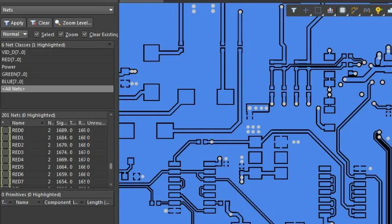
Another critical factor for inner layers is impedance control. In high-speed designs, traces on inner layers often carry sensitive signals, and maintaining consistent spacing is vital to avoid impedance mismatches. For example, a differential pair on an inner layer might require a specific spacing (e.g., 8 mils or 0.008 inches) to achieve a target impedance of 100 ohms, depending on the dielectric material and trace width.
Factors Affecting Inner Layer Spacing
- Signal Integrity: High-speed signals on inner layers are more prone to crosstalk due to proximity to other traces. Controlled spacing helps maintain signal quality.
- Heat Dissipation: Inner layers have less access to airflow, so tighter spacing can lead to localized heating, especially in power-heavy designs.
- Manufacturing Challenges: Inner layers go through lamination under high pressure and temperature (often around 375°F and 275-400 psi). Small spacing errors can lead to shorts or defects that are hard to detect.
Key Differences Between Inner and Outer Layer Trace Spacing
While both inner and outer layers follow similar principles for trace spacing, there are notable differences in how these rules are applied during PCB manufacturing and design. Here's a quick comparison:
| Aspect | Outer Layers | Inner Layers |
|---|---|---|
| Exposure | Exposed to environment, covered by solder mask | Enclosed within insulating layers |
| Typical Minimum Spacing | 6 mils (0.006 inches) for low voltage | 5-6 mils (0.005-0.006 inches) for low voltage |
| Inspection | Easier to inspect and repair | Harder to inspect, defects may go unnoticed |
| Signal Integrity Focus | Less critical for high-speed signals | More critical due to controlled impedance needs |
Understanding these differences helps designers make informed decisions when laying out traces on different PCB layers. For instance, you might prioritize tighter spacing on inner layers for high-density designs but increase spacing on outer layers for high-voltage applications.
Industry Standards and Guidelines for Trace Spacing
To ensure reliability and safety, PCB designers often follow industry standards when determining minimum trace spacing. One of the most widely used standards is IPC-2221, which provides detailed guidelines based on voltage, layer type, and application.
For example, IPC-2221 suggests the following minimum spacing for conductors on the same layer:
- 0-50V: 6 mils (0.006 inches or 0.152 mm)
- 51-100V: 12 mils (0.012 inches or 0.305 mm)
- 101-300V: 30 mils (0.030 inches or 0.762 mm)
These values are starting points and may need adjustment based on specific design requirements, such as high-speed signal needs or environmental conditions. Always consult the latest standards or work with your manufacturing partner to confirm the best spacing for your project.
Practical Tips for Designing Trace Spacing
Now that we've covered the basics of trace spacing for different PCB layers, here are some actionable tips to help you apply this knowledge effectively in your designs:
- Know Your Voltage Requirements: Always check the operating voltage of your circuit and apply the appropriate spacing to prevent arcing or breakdown.
- Consider Signal Speed: For high-speed designs, especially on inner layers, maintain consistent spacing to control impedance and minimize crosstalk. Tools like impedance calculators can help determine exact spacing for differential pairs.
- Account for Manufacturing Limits: Work closely with your PCB manufacturer to understand their minimum spacing capabilities. Some may handle 4 mils (0.004 inches) spacing, while others might require 6 mils (0.006 inches) or more.
- Use Design Software Rules: Most PCB design software allows you to set minimum spacing rules for different layers. Use these features to catch spacing errors early in the design process.
- Test and Validate: After designing, simulate your PCB layout to check for signal integrity issues or potential manufacturing problems related to spacing.
Common Mistakes to Avoid with Trace Spacing
Even experienced designers can make mistakes when it comes to trace spacing. Here are some pitfalls to watch out for:
- Ignoring Voltage Ratings: Underestimating voltage levels can lead to insufficient spacing, risking shorts or arcing.
- Overlooking Layer Differences: Applying the same spacing rules to inner and outer layers without considering their unique constraints can cause design flaws.
- Pushing Manufacturing Limits: Designing with spacing below your manufacturer’s capabilities can result in production delays or defects.
- Neglecting Signal Integrity: Tight spacing might save board space but can degrade signal quality, especially in high-speed circuits.
Conclusion: Mastering Trace Spacing for Better PCB Design
Understanding minimum trace spacing for different PCB layers is a fundamental skill for any designer or engineer. Whether you're working on the outer layers, exposed to environmental factors, or the inner layers, critical for signal integrity, getting the spacing right ensures your board is safe, reliable, and manufacturable. By considering factors like voltage, signal speed, and manufacturing constraints, and by following industry standards, you can create designs that perform well in any application.
At ALLPCB, we’re committed to supporting your PCB projects with high-quality manufacturing services tailored to your design needs. Whether you’re tackling a simple two-layer board or a complex multilayer design, mastering trace spacing is a step toward success. Keep these guidelines in mind for your next project, and you’ll be on your way to creating robust, efficient PCBs.


