ALLPCB


If you're dealing with HASL defects like solder bridging, uneven coating, pinholes, or dewetting in your PCB manufacturing process, you're not alone. These issues can compromise the quality and reliability of your boards, leading to costly rework or failures. In this comprehensive guide, we'll walk you through the most common HASL (Hot Air Solder Leveling) defects, their causes, and practical solutions to troubleshoot and prevent them. Whether you're a seasoned engineer or new to PCB assembly, this post will equip you with actionable tips to improve your process and achieve consistent, high-quality results.
What is HASL and Why Does It Matter?
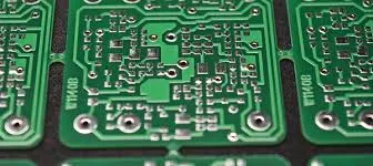
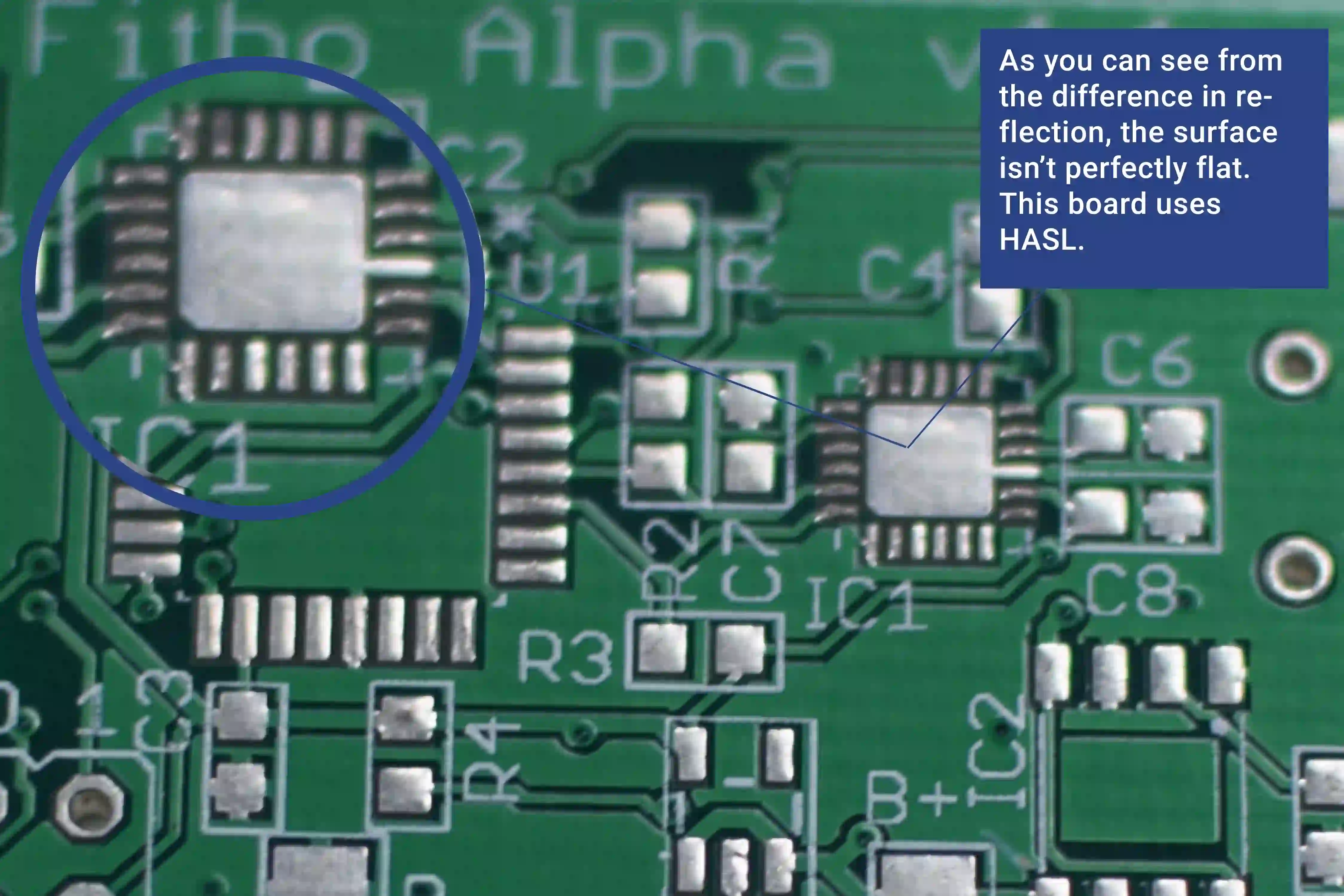
HASL, or Hot Air Solder Leveling, is a widely used surface finish in PCB manufacturing. It involves dipping the board into molten solder and then using hot air knives to remove excess solder, leaving a thin, even coating on the copper pads. This finish is popular due to its cost-effectiveness and excellent solderability, making it ideal for many applications. However, despite its advantages, HASL is prone to certain defects that can affect the performance of the final product.
Understanding and troubleshooting these defects is crucial because they can lead to poor solder joint reliability, assembly issues, and even complete board failures. By addressing problems like solder bridging, uneven coating, pinholes, and dewetting early, you can save time, reduce rework costs, and ensure your boards meet industry standards.
Common HASL Defects and Their Causes
Before diving into solutions, let’s explore the most frequent HASL defects, their root causes, and how they impact PCB performance. Identifying the source of the problem is the first step to effective troubleshooting.
1. Solder Bridging
Solder bridging occurs when excess solder creates an unintended connection between two adjacent pads or traces, leading to short circuits. This defect is often visible as a small blob or line of solder spanning across components.
Causes:
- Improper hot air knife settings, such as low air pressure or incorrect angle, which fail to remove excess solder.
- Board design issues, like pads or traces placed too closely together (less than 0.2 mm spacing in some cases).
- Contaminated solder bath with impurities that affect solder flow.
Impact: Solder bridging can cause electrical shorts, rendering the PCB unusable and requiring manual rework, which increases production time and costs.
2. Uneven Coating
Uneven coating refers to inconsistent solder thickness across the PCB surface. Some areas may have thick solder buildup, while others appear thin or bare.
Causes:
- Inconsistent immersion time in the solder bath, leading to uneven solder deposition.
- Hot air knife misalignment or uneven air distribution during leveling.
- Poor board flatness or warpage, causing solder to pool in certain areas.
Impact: Uneven coating can lead to weak solder joints, affecting component attachment and long-term reliability. It may also cause issues during assembly, as components may not sit flush on the board.
3. Pinholes
Pinholes are small, visible holes or voids in the solder coating on the PCB pads. These defects expose the underlying copper, making it vulnerable to oxidation.
Causes:
- Contamination on the board surface, such as dust or oil, preventing proper solder adhesion.
- Inadequate flux application, which fails to clean the copper surface before soldering.
- Excessive air entrapment during the HASL process, creating voids in the coating.
Impact: Pinholes reduce solderability and increase the risk of corrosion, leading to potential failures over time, especially in harsh environments.
4. Dewetting
Dewetting happens when solder fails to adhere to the copper surface, pulling back to form uneven or incomplete coverage. It often looks like small, irregular patches of exposed copper.
Causes:
- Oxidation or contamination on the copper surface before the HASL process.
- Improper flux activity or insufficient preheating, which hinders solder wetting.
- Solder bath temperature issues, such as being too low (below 250°C), which prevents proper flow.
Impact: Dewetting compromises solder joint strength, leading to poor component connections and potential failures during operation.
Practical Solutions for Troubleshooting HASL Defects
Now that we’ve identified the common HASL defects and their causes, let’s dive into actionable solutions to troubleshoot and prevent these issues. These tips are designed to help you optimize your process and achieve consistent results.
Troubleshooting Solder Bridging
To eliminate solder bridging, focus on both process adjustments and design considerations:
- Optimize Hot Air Knife Settings: Ensure the air pressure is set between 3-5 psi and the angle of the knives is around 45 degrees to effectively remove excess solder. Regularly inspect and clean the knives to prevent blockages.
- Review Board Design: Maintain a minimum pad spacing of 0.2 mm for fine-pitch components. Use design software to simulate solder flow and identify potential bridging risks before production.
- Maintain Solder Bath Purity: Regularly test and filter the solder bath to remove impurities. Replace the solder if dross levels exceed 1% of the total volume.
Fixing Uneven Coating
Addressing uneven coating requires precise control over the HASL process parameters:
- Control Immersion Time: Standardize the immersion time in the solder bath to 2-4 seconds to ensure uniform solder deposition. Use automated equipment for consistency.
- Calibrate Hot Air Knives: Check the alignment and pressure distribution of the air knives. Ensure uniform airflow across the board by adjusting the knife position if needed.
- Inspect Board Flatness: Use a flatness tester to measure board warpage before the HASL process. Boards with warpage exceeding 0.75% of the diagonal length should be corrected or rejected.
Eliminating Pinholes
Preventing pinholes involves maintaining a clean process environment and proper preparation:
- Clean the Board Surface: Use a thorough pre-cleaning process with isopropyl alcohol or a dedicated PCB cleaner to remove contaminants like oil or dust before fluxing.
- Optimize Flux Application: Apply flux evenly using a spray or foam method to ensure complete coverage. Use a flux with a solids content of 2-3% for best results.
- Minimize Air Entrapment: Reduce turbulence in the solder bath by maintaining a stable immersion speed of 1-2 feet per second. Consider using nitrogen blanketing to minimize oxidation.
Preventing Dewetting
Dewetting can be avoided by ensuring proper surface preparation and temperature control:
- Prevent Copper Oxidation: Store bare copper boards in a controlled environment with low humidity (below 50%) and apply a protective coating if delays occur before HASL processing.
- Adjust Preheat and Solder Temperatures: Preheat the board to 100-120°C before immersion to remove moisture and activate flux. Maintain the solder bath temperature between 250-260°C for optimal wetting.
- Use Effective Flux: Select a flux with strong oxide removal properties and test its performance regularly. Replace flux if it shows signs of degradation.
HASL Rework: Tips for Correcting Defects
Sometimes, despite best efforts, defects slip through, and rework becomes necessary. HASL rework can be challenging due to the risk of damaging the board or worsening the defect. Here are practical tips for effective rework:
- Solder Bridging Rework: Use a fine-tip soldering iron (set to 300°C) and desoldering wick to carefully remove excess solder between pads. Clean the area with isopropyl alcohol and a brush to remove residue.
- Uneven Coating Correction: For minor unevenness, apply a small amount of flux and touch up with a soldering iron to redistribute solder. For severe cases, consider stripping the HASL layer using a chemical stripper and reapplying the finish.
- Pinhole Repair: Apply flux to the affected area and use a soldering iron to add a thin layer of solder over the pinhole. Ensure the added solder blends seamlessly with the existing coating.
- Dewetting Fix: Clean the dewetted area with flux and alcohol to remove oxidation, then reapply solder using a soldering iron. If dewetting persists, inspect the board for underlying copper quality issues.
Caution: Limit rework cycles to avoid thermal stress on the board, which can cause delamination or pad lifting. Ideally, keep rework attempts to a maximum of two per area.
Preventive Measures for Long-Term Success
While troubleshooting and rework are essential, prevention is always better than correction. Implementing these long-term strategies can minimize HASL defects and improve overall process reliability:
- Regular Equipment Maintenance: Schedule monthly checks on HASL equipment, including solder bath temperature sensors, hot air knives, and conveyor systems, to ensure consistent performance.
- Process Monitoring: Use real-time monitoring tools to track parameters like immersion time, air pressure, and bath temperature. Set alarms for deviations beyond ±5% of target values.
- Staff Training: Train operators on proper HASL techniques and defect identification. Conduct quarterly refreshers to keep skills sharp and introduce updates to processes.
- Quality Control Checks: Implement visual and automated optical inspection (AOI) after the HASL process to catch defects early. Target a defect rate of less than 0.5% for critical applications.
Conclusion: Mastering HASL for Reliable PCBs
Troubleshooting HASL defects like solder bridging, uneven coating, pinholes, and dewetting is a critical skill for anyone involved in PCB manufacturing. By understanding the causes of these issues and applying the practical solutions outlined in this guide, you can significantly improve the quality and reliability of your boards. From optimizing process parameters to mastering rework techniques, every step you take toward defect prevention saves time, reduces costs, and enhances your final product.
At ALLPCB, we’re committed to supporting engineers and manufacturers with resources and expertise to tackle challenges like HASL defects. With the right approach and attention to detail, you can achieve consistent, high-quality results in your PCB projects. Keep refining your process, and don’t hesitate to reach out for expert guidance on your next project.