ALLPCB


 Overview
TTL transistor switch circuits are classified by drive capability into small-signal switches and power switches. By transistor connection they are classified into emitter-grounded switches (PNP transistor emitter connected to supply) and emitter-follower switch circuits.
1. Emitter-grounded switch circuits
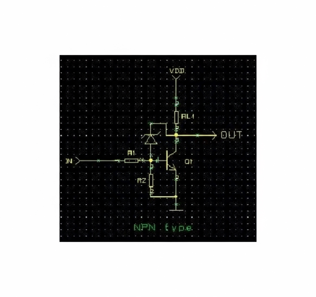
1.1 Basic NPN and PNP switch diagrams
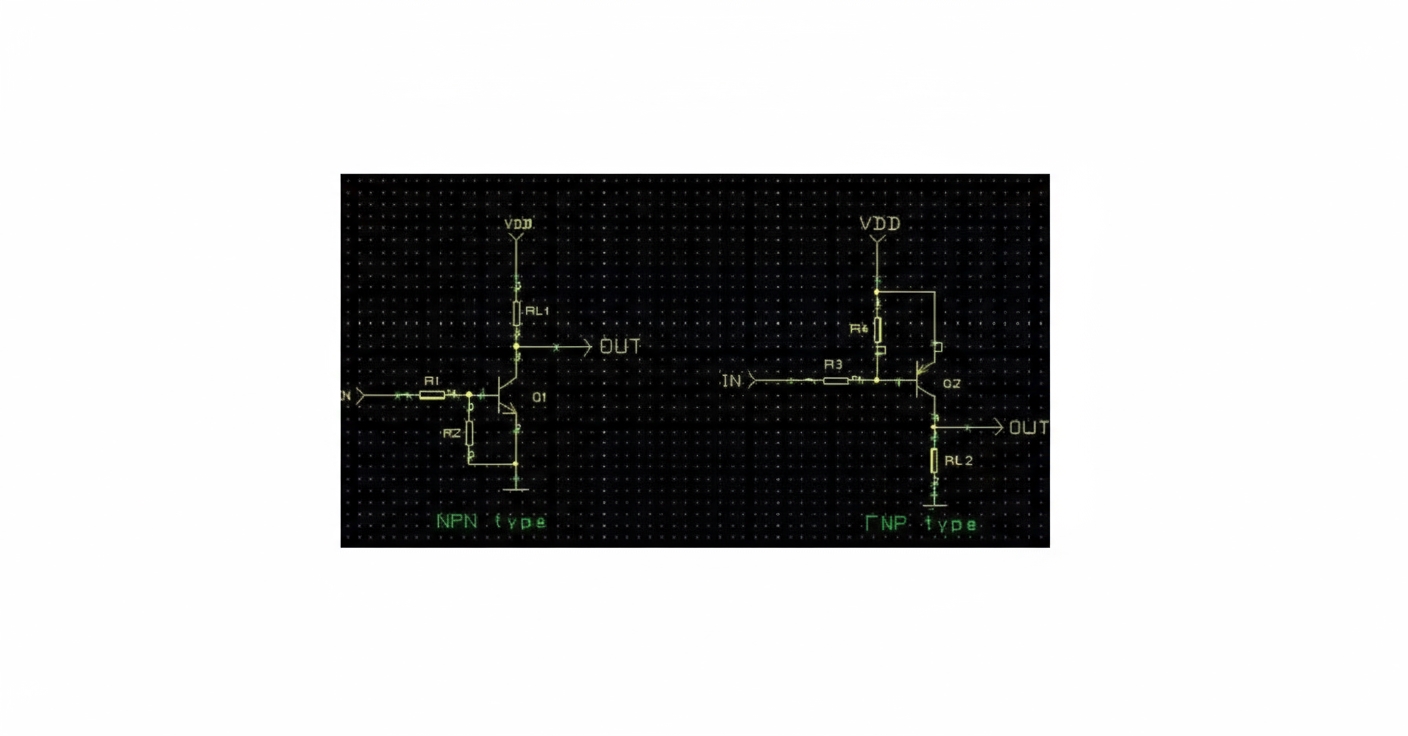
The basic circuits above differ from practical designs in that transistor base charge storage causes a transition period from on to off. When the transistor turns off, the presence of R1 slows base-charge removal, so Ic does not immediately drop to zero. In other words, emitter-grounded switch circuits have a turn-off delay and are not suitable for direct use in mid-to-high-frequency switching.
1.2 Practical NPN and PNP switch with speed-up capacitor
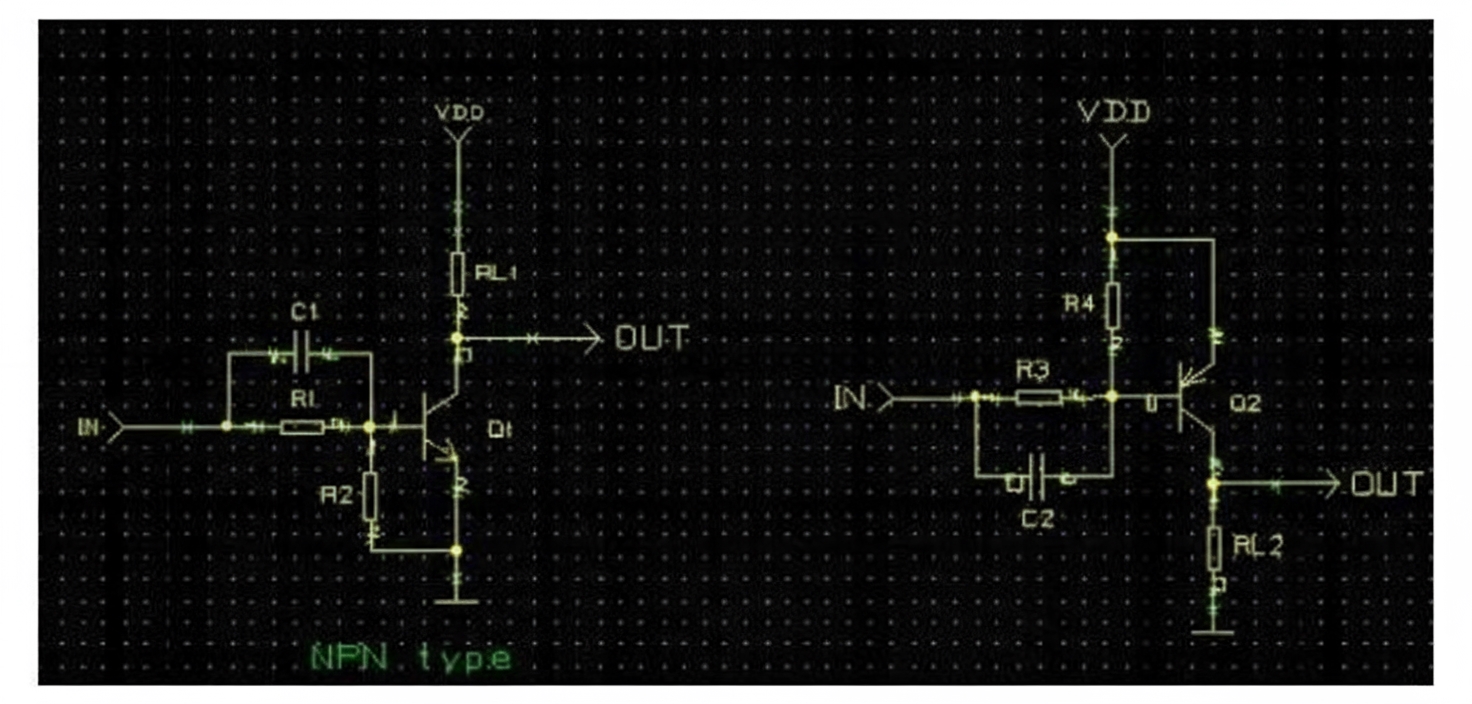
Explanation: When the transistor is driven rapidly into conduction (IN changes abruptly), C1 momentarily shorts and supplies base current to the transistor, accelerating turn-on. When the transistor is driven rapidly toward cutoff (IN changes abruptly), C1 again provides a momentary low-impedance path to discharge base charge, accelerating turn-off. C is typically tens to hundreds of picofarads. R2 ensures the transistor remains off when IN is not driven high; R4 ensures the transistor remains off when IN is not driven low. R1 and R3 limit base current.
1.3 Practical NPN switch with Schottky clamp
Explanation: Because a Schottky diode forward voltage Vf is about 0.2 to 0.4 V, which is lower than Vbe, when the transistor conducts most of the base current flows through the diode and then through the transistor to ground. This reduces the base current flowing into the transistor and thus reduces accumulated charge. When the transistor turns off, the smaller stored charge requires less time to remove, so turn-off is faster.
1.4 Practical design considerations
In practical design ensure transistor Vceo and Vcbo ratings meet voltage requirements, and the transistor satisfies collector power dissipation. Calculate the base resistor from the load current and hFE (use the transistor minimum hFE for calculations) and provide a margin of 0.5 to 1 times the required base current. Note the Schottky diode reverse voltage rating.
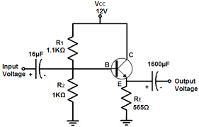
Transistor Switch Circuit
Besides being used as AC signal amplifiers, transistors can function as switches. Strictly speaking, a transistor does not operate identically to a mechanical contact switch, but it offers characteristics mechanical switches do not. Figure 1 shows a basic electronic transistor switch circuit.
The load resistor is connected between the supply and the transistor collector and lies in the main current path of the transistor.
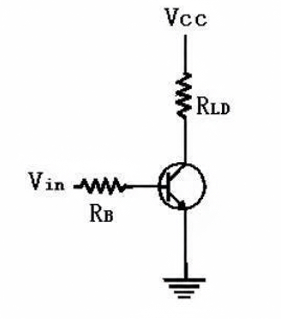
Figure 1: Basic transistor switch
Input voltage Vin controls the transistor switch open and closed states. When the transistor is open, load current is blocked. When the transistor is closed, current flows. Specifically, when Vin is low, no base current flows, so no collector current flows and the load connected to the collector has no current, which corresponds to the switch being open; the transistor is in cutoff. Conversely, when Vin is high, base current flows and the collector conducts a larger, amplified current, so the load circuit is driven; this corresponds to the switch being closed and the transistor operating in saturation.
Analysis and design of transistor switch circuits
For silicon transistors, the base-emitter forward voltage is about 0.6 V. To ensure the transistor is in cutoff, Vin must be below about 0.6 V so base current is zero. In practice, designers often use Vin below 0.3 V to be certain the transistor is cutoff. The closer Vin is to 0 V, the more certain the transistor remains cutoff.
To transfer current to the load, the transistor collector-emitter must be effectively shorted, analogous to a closed mechanical switch. This requires Vin to be high enough to drive the transistor into saturation. In saturation, collector current is high and nearly the entire supply voltage Vcc appears across the load resistor, making Vce approach 0 so the collector and emitter are nearly short-circuited.
The above expresses the basic relationship between IC and IB, where beta represents the transistor DC current gain. For some transistors the AC beta and DC beta differ significantly. To ensure the switch closes, Vin must be high enough to provide the minimum base current required by the previous relation.
Once the base voltage exceeds the value from the above equation, the transistor conducts and nearly the entire supply voltage appears across the load, completing the closed-switch action.
In summary, when a transistor is connected as in Figure 1, it functions similarly to a mechanical switch in series with the load. The switching can be controlled directly by an input voltage instead of mechanical actuators, solenoid plungers, or relay armatures.
For clarity, the transistor switches discussed here use NPN transistors, although PNP transistors can also be used as switches.