 ALLPCB


In today’s electronics world, lead-free PCB assembly services are more important than ever. If you’re looking for reliable solutions for lead-free SMT assembly or lead-free PTH assembly, you’ve come to the right place. This guide will walk you through everything you need to know about lead-free PCB assembly, from its benefits and challenges to the processes involved. Whether you’re an engineer, a product designer, or a business owner, you’ll find practical insights to help you make informed decisions for your projects.
At its core, lead-free PCB assembly means creating printed circuit boards without using lead-based solder or materials. This is driven by environmental and health regulations, like RoHS (Restriction of Hazardous Substances), which limit the use of harmful substances in electronics. In the sections below, we’ll dive deep into the details of lead-free assembly, covering both Surface Mount Technology (SMT) and Plated Through-Hole (PTH) methods, to ensure you have a complete understanding.
Why Choose Lead-Free PCB Assembly?
Lead-free PCB assembly isn’t just a trend—it’s a necessity for many industries. Lead, once a common material in soldering, poses significant health and environmental risks. When electronics are discarded, lead can leach into soil and water, causing harm. For workers, exposure to lead during manufacturing can lead to serious health issues. That’s why regulations like RoHS, introduced in the European Union in 2006, restrict lead content to less than 0.1% in electronic components.
Opting for lead-free assembly offers several benefits:
- Compliance with Global Standards: Many countries require lead-free electronics for import and sale. Using lead-free assembly ensures your products meet these legal requirements.
- Environmental Responsibility: Reducing hazardous materials helps protect the planet and aligns with corporate sustainability goals.
- Safer Working Conditions: Lead-free processes minimize health risks for workers handling materials during production.
- Market Competitiveness: Consumers and businesses often prefer eco-friendly products, giving you an edge in the market.
Understanding Lead-Free SMT Assembly
Lead-free SMT assembly refers to the process of mounting components directly onto the surface of a printed circuit board using lead-free solder. Surface Mount Technology (SMT) is the most widely used method in modern electronics because it allows for smaller, lighter, and more efficient designs. However, switching to lead-free materials in SMT assembly comes with unique considerations.
Key Materials in Lead-Free SMT Assembly
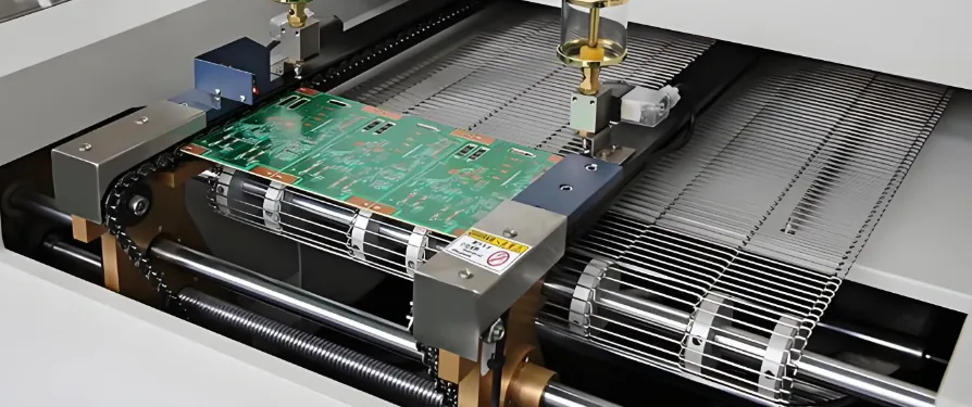
The primary difference in lead-free SMT assembly is the type of solder used. Traditional tin-lead solder has been replaced with alternatives like SAC305, a common lead-free alloy made of 96.5% tin, 3% silver, and 0.5% copper. This alloy has a higher melting point, typically around 217-220°C, compared to 183°C for tin-lead solder. This means that the reflow ovens used in SMT assembly must operate at higher temperatures, often between 240-260°C, to ensure proper soldering.
Other materials, such as PCB surface finishes, also play a role. Lead-free compatible finishes like Immersion Silver, ENIG (Electroless Nickel Immersion Gold), and OSP (Organic Solderability Preservative) are often used to ensure good solderability and reliability.
Challenges in Lead-Free SMT Assembly
While lead-free SMT assembly is beneficial, it does present some challenges:
- Higher Temperatures: The increased reflow temperatures can stress components and PCB substrates, potentially leading to thermal damage if not managed properly.
- Cost: Lead-free solder materials, like those containing silver, are often more expensive than traditional options.
- Reliability Concerns: Lead-free solder joints can be more brittle, increasing the risk of cracking under mechanical stress or thermal cycling.
Despite these challenges, advancements in technology and process control have made lead-free SMT assembly highly reliable for most applications, from consumer electronics to industrial equipment.
Exploring Lead-Free PTH Assembly
Lead-free PTH assembly, or Plated Through-Hole assembly, involves inserting component leads through holes in the PCB and soldering them on the opposite side using lead-free solder. While SMT dominates modern PCB design, PTH assembly is still used for components that require extra mechanical strength, such as connectors, transformers, and large capacitors.
Lead-Free Soldering in PTH Assembly
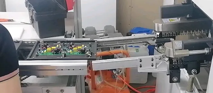
In lead-free PTH assembly, the soldering process often uses wave soldering or selective soldering techniques. Wave soldering involves passing the PCB over a wave of molten lead-free solder, typically SAC305, at temperatures around 260°C. Selective soldering, on the other hand, targets specific areas of the board, reducing thermal stress on sensitive components.
The higher melting point of lead-free solder requires careful control of the soldering temperature and duration to prevent damage to the PCB or components. For instance, prolonged exposure to temperatures above 260°C can cause delamination of the PCB substrate or degradation of component insulation.
Advantages of Lead-Free PTH Assembly
Lead-free PTH assembly offers specific advantages, especially for applications requiring durability:
- Stronger Mechanical Bonds: Through-hole soldering creates robust connections that withstand vibration and mechanical stress, ideal for automotive and industrial applications.
- Compatibility with High-Power Components: Many high-power or high-heat components are designed for through-hole mounting, and lead-free options ensure compliance with regulations.
However, similar to SMT, the higher temperatures and material costs can pose challenges. Proper equipment calibration and operator training are essential to achieve consistent results.
Key Differences Between Lead-Free SMT and PTH Assembly
Understanding the differences between lead-free SMT assembly and lead-free PTH assembly can help you choose the right method for your project. Here’s a quick comparison:
| Aspect | Lead-Free SMT Assembly | Lead-Free PTH Assembly |
|---|---|---|
| Component Placement | Surface-mounted on PCB | Inserted through holes in PCB |
| Soldering Method | Reflow soldering in ovens | Wave or selective soldering |
| Typical Applications | Small, compact electronics like smartphones | High-power, durable components like connectors |
| Thermal Stress | Higher risk due to reflow temperatures (240-260°C) | Localized heat, but still high (around 260°C) |
Both methods require precise control to handle the characteristics of lead-free solder, but they serve different purposes based on the design and requirements of the PCB.
Best Practices for Lead-Free PCB Assembly
To ensure high-quality results in both SMT and PTH lead-free assembly, consider these best practices:
1. Use Compatible Materials
Choose components, solder pastes, and PCB finishes that are designed for lead-free processes. For instance, ensure that the PCB laminate can withstand temperatures up to 260°C without degrading. Common laminates like FR-4 with higher Tg (glass transition temperature) values of 170°C or more are often recommended.
2. Optimize Thermal Profiles
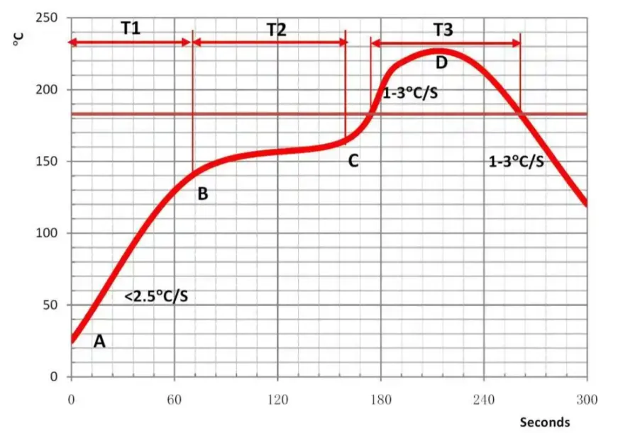
For SMT assembly, create a reflow profile with four key zones: preheat (to 150-180°C), soak (to stabilize temperatures), reflow (peak at 240-260°C), and cooling. Each zone should be carefully timed—typically, the reflow zone lasts 30-90 seconds—to avoid thermal shock. For PTH, adjust wave soldering parameters to minimize dwell time in the solder wave, ideally under 5 seconds.
3. Invest in Quality Equipment
Modern reflow ovens and wave soldering machines with precise temperature control are critical for lead-free assembly. Equipment should support nitrogen atmospheres in reflow ovens to reduce oxidation of lead-free solder, improving joint quality.
4. Train Your Team
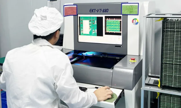
Lead-free assembly requires specific skills, especially in handling higher temperatures and brittle solder joints. Regular training on process control and inspection techniques, such as X-ray imaging for hidden solder joints, can prevent defects.
Common Challenges and Solutions in Lead-Free Assembly
Transitioning to lead-free PCB assembly can come with hurdles, but there are proven solutions to address them:
- Issue: Tombstoning in SMT Assembly – This occurs when one end of a component lifts during reflow due to uneven heating. Solution: Optimize the reflow profile and ensure uniform pad design to balance solder wetting.
- Issue: Brittle Solder Joints – Lead-free solder can crack under stress. Solution: Use underfill materials or reinforce joints in high-stress areas.
- Issue: Component Damage from Heat – High temperatures can degrade sensitive components. Solution: Select components rated for lead-free processes and shield sensitive areas during soldering.
Why Partner with a Trusted PCB Assembly Service?
Navigating the complexities of lead-free PCB assembly—whether it’s lead-free SMT assembly or lead-free PTH assembly—requires expertise and advanced equipment. Partnering with a trusted service provider ensures access to the latest technology, skilled technicians, and strict quality control measures. From prototype to mass production, a reliable assembly service can help you meet regulatory standards, reduce costs through optimized processes, and deliver high-quality products on time.
Look for a provider that offers:
- RoHS-compliant materials and processes.
- Advanced inspection tools like Automated Optical Inspection (AOI) and X-ray systems.
- Customizable solutions for both SMT and PTH assembly needs.
Future Trends in Lead-Free PCB Assembly
As technology evolves, so does the landscape of lead-free PCB assembly. Here are some trends to watch in 2025 and beyond:
- Automation and AI: Automated SMT lines with AI-driven defect detection are becoming standard, improving precision and reducing errors in lead-free assembly.
- Green Manufacturing: Beyond lead-free, the industry is moving toward fully sustainable practices, including recyclable materials and energy-efficient processes.
- Miniaturization: As devices get smaller, lead-free SMT assembly will need to adapt to tighter tolerances and finer pitch components, requiring even more precise equipment.
Staying ahead of these trends can position your business for success in a rapidly changing market.
Conclusion
Lead-free PCB assembly is a critical step toward safer, more sustainable electronics manufacturing. Whether you’re focused on lead-free SMT assembly for compact, high-density designs or lead-free PTH assembly for robust, high-power applications, understanding the processes, challenges, and best practices is essential. By choosing the right materials, optimizing thermal profiles, and partnering with a trusted assembly service, you can achieve high-quality results that meet global standards.
This guide has covered the essentials to help you navigate the world of lead-free assembly. With the right knowledge and resources, you can ensure your projects are compliant, reliable, and ready for the future of electronics manufacturing.


