In the fast-evolving world of electronics, designing high-current PCBs that handle significant power while minimizing size is a critical challenge. One of the most effective strategies to achieve this balance is through the use of embedded components in PCB design. This approach not only saves space but also enhances thermal management and performance in high-power applications. In this blog, we’ll dive deep into how embedded components can revolutionize high-current PCB design, focusing on space-saving solutions, thermal conductivity, high-density techniques, and cost considerations.
Why Embedded Components Matter in High-Current PCB Design
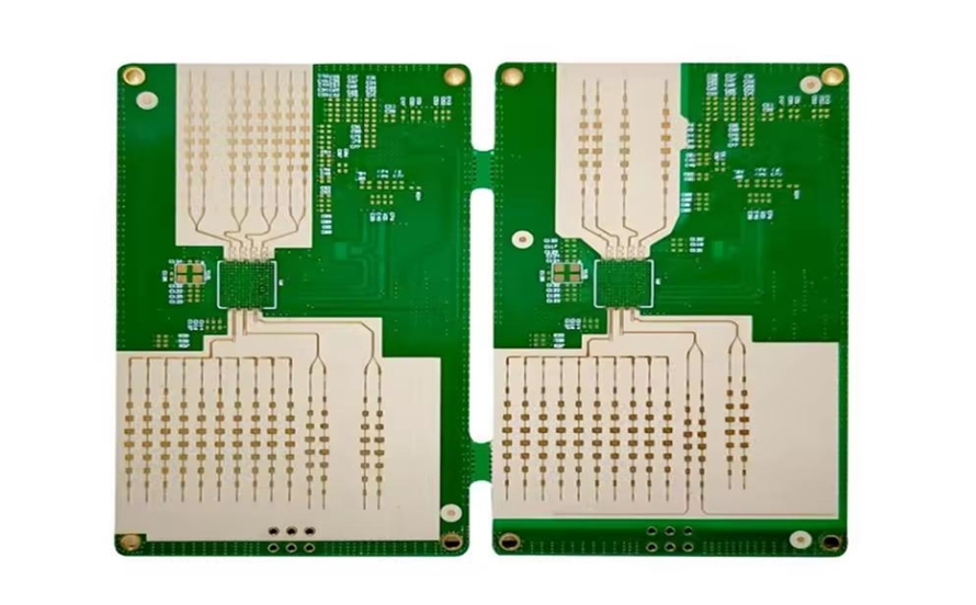
Embedded components are parts like resistors, capacitors, and even active devices that are integrated directly into the layers of a printed circuit board (PCB) rather than mounted on its surface. This technique is a game-changer for high-current PCB designs where space is limited, and power demands are high. By embedding components, you can reduce the PCB footprint, improve signal integrity, and enhance thermal performance—an essential trio for modern electronics.
For engineers working on compact devices such as power supplies, automotive electronics, or industrial controllers, minimizing PCB size in high-power applications is often a top priority. Embedded components offer a direct solution by freeing up surface space and allowing for tighter, more efficient layouts. Let’s explore how this works in detail.
Key Benefits of Embedded Components in High-Current PCB Design
Using embedded components in high-current PCB design brings several advantages that directly address the challenges of space, power, and heat. Here are the standout benefits:
1. Space-Saving Design for Minimizing PCB Size in High-Power Applications
In high-power systems, traditional surface-mounted components can take up valuable real estate on the PCB. Embedding components within the board’s layers eliminates the need for surface space, allowing for a smaller overall footprint. For instance, in a power converter design, embedding capacitors and resistors can reduce the board size by up to 30%, depending on the complexity of the circuit. This is crucial for applications like wearable devices or compact power modules where every millimeter counts.
Additionally, a smaller PCB means shorter trace lengths, which can reduce parasitic inductance and resistance—key factors in maintaining efficiency in high-current designs. Shorter traces can lower impedance by as much as 10-15% in some layouts, leading to better power delivery.
2. Improved Thermal Conductivity with Embedded Components
High-current applications generate significant heat, and managing this heat is vital for reliability and performance. Embedded components can be placed closer to heat-dissipating layers or thermal vias within the PCB, improving heat transfer. For example, embedding a power resistor near a copper plane can enhance thermal conductivity by up to 20% compared to surface mounting, as the heat spreads more evenly across the board.
Materials like high-thermal-conductivity substrates (often with values around 1-2 W/m·K) can be paired with embedded components to further optimize heat dissipation. This setup is ideal for applications like LED drivers or motor controllers, where overheating can lead to failure.
3. Enhanced High-Density PCB Design Techniques
Embedding components supports high-density PCB design by allowing more functionality in a smaller area. This technique pairs well with other high-density interconnect (HDI) methods, such as microvias and fine-pitch traces, to create compact yet powerful boards. For instance, in a multi-layer PCB, embedded capacitors can be placed directly under power ICs, reducing noise and improving signal integrity at frequencies up to 1 GHz or higher.
This approach also minimizes the need for external connections, cutting down on potential points of failure. In high-current designs, where reliability is non-negotiable, this can be a significant advantage for industries like aerospace or medical electronics.
How to Implement Embedded Components in High-Current PCB Design
Integrating embedded components into a high-current PCB requires careful planning and execution. Below are actionable steps to ensure success, tailored for engineers looking to optimize space and performance.
Step 1: Select the Right Components for Embedding
Not all components are suitable for embedding. Passive components like resistors and capacitors are the most common choices due to their small size and compatibility with PCB manufacturing processes. For high-current designs, prioritize components with high power ratings (e.g., resistors handling 5W or more) and ensure they can withstand the heat generated during operation.
Active components, such as transistors or small ICs, can also be embedded in some cases, especially with advanced techniques like die embedding. However, these require specialized manufacturing processes and may increase costs.
Step 2: Optimize Layer Stack-Up for Thermal and Electrical Performance
In a high-current PCB, the layer stack-up plays a critical role in managing heat and power distribution. Place embedded components in inner layers close to ground or power planes to minimize noise and improve thermal conductivity. For example, a 6-layer PCB might have embedded capacitors in layer 3, directly below a power IC on layer 1, to reduce loop inductance by up to 25%.
Use thicker copper layers (e.g., 2 oz or 70 μm) for high-current paths to handle loads of 10A or more without excessive heat buildup. Pair this with thermal vias to channel heat away from critical areas.
Step 3: Leverage Advanced Manufacturing Techniques
Embedding components often requires advanced PCB fabrication techniques, such as laser drilling for microvias or cavity formation for larger components. Work closely with your manufacturing partner to ensure the process aligns with your design goals. For high-density PCB design, consider HDI technology to achieve finer traces (down to 3 mil or 75 μm) and smaller vias, maximizing space efficiency.
Cost Analysis of Embedded PCB Designs
While embedded components offer clear benefits for high-current PCB design, they can impact costs. Understanding these trade-offs is essential for making informed decisions. Let’s break down the key cost factors.
Initial Design and Manufacturing Costs
Embedding components typically increases upfront costs due to the complexity of the design and manufacturing process. For example, creating cavities or integrating components into inner layers may raise fabrication costs by 15-30% compared to a standard PCB. Specialized equipment and tighter tolerances also contribute to higher expenses.
However, for high-volume production, these costs can be offset by the reduced need for external components and smaller board sizes, which lower material expenses over time.
Long-Term Savings and Performance Gains
The long-term benefits of embedded PCBs often outweigh the initial investment. Smaller boards mean less material usage, and improved thermal performance can extend the lifespan of the product, reducing warranty or replacement costs. For instance, a high-current power module with embedded components might achieve a 10% higher efficiency, translating to energy savings in applications like industrial automation.
Additionally, fewer surface-mounted parts mean reduced assembly time and lower risk of soldering defects, further cutting costs in large-scale production.
Challenges and Solutions in Using Embedded Components
Despite their advantages, embedded components come with challenges that engineers must address to ensure a successful design.
Challenge 1: Design Complexity
Embedding components adds layers of complexity to the design process. Placement must be precise to avoid interference with other elements, and simulation tools are often needed to predict thermal and electrical behavior. Use advanced design software to model the impact of embedded components on signal integrity and heat dissipation before manufacturing.
Challenge 2: Repair and Maintenance
Unlike surface-mounted components, embedded parts are difficult or impossible to replace if they fail. To mitigate this, focus on rigorous testing during the design phase to ensure reliability. Select components with proven durability for high-current environments, and consider redundancy for critical functions.
Challenge 3: Thermal Management Limitations
While embedding can improve thermal conductivity, it can also trap heat in inner layers if not managed properly. Incorporate thermal vias and heat sinks into the design to dissipate heat effectively. For high-power designs handling currents above 20A, consider hybrid approaches that combine embedded components with external cooling solutions.
Real-World Applications of Embedded Components in High-Current PCBs
Embedded components are already making a significant impact in various industries. Here are a few examples of how they’re used in high-current designs:
- Automotive Electronics: In electric vehicles, embedded components help create compact power control units that manage currents of 50A or more while fitting into tight spaces.
- Industrial Power Supplies: High-density PCBs with embedded capacitors and resistors ensure stable power delivery in harsh environments, with designs handling up to 100W of power dissipation.
- Consumer Electronics: Compact devices like smartphones use embedded passives to save space and improve battery efficiency, even under high-current charging conditions.
Future Trends in Embedded Component Technology
The field of embedded components is advancing rapidly, with new materials and techniques on the horizon. Innovations like 3D embedding, where components are stacked vertically within the PCB, promise even greater space savings. Additionally, the integration of wide-bandgap semiconductors like GaN and SiC into embedded designs is set to boost efficiency in high-power applications, potentially increasing power density by 40% or more.
As manufacturing costs decrease and design tools become more accessible, we expect embedded components to become a standard in high-current PCB design, especially for industries pushing the boundaries of miniaturization and performance.
Conclusion: Unlocking the Potential of Embedded Components
High-current PCB design with embedded components offers a powerful solution for engineers looking to save space, enhance thermal conductivity, and achieve high-density layouts. By minimizing PCB size in high-power applications, this approach meets the demands of modern electronics without compromising performance. While there are cost and complexity considerations, the long-term benefits—such as improved reliability and reduced material usage—make embedded components a smart choice for many projects.
Whether you’re designing for automotive, industrial, or consumer applications, leveraging embedded components can give your high-current PCB designs a competitive edge. With careful planning and the right manufacturing support, you can unlock the full potential of this space-saving technology.
 ALLPCB


