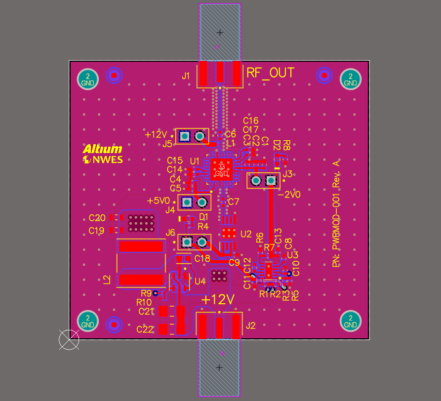
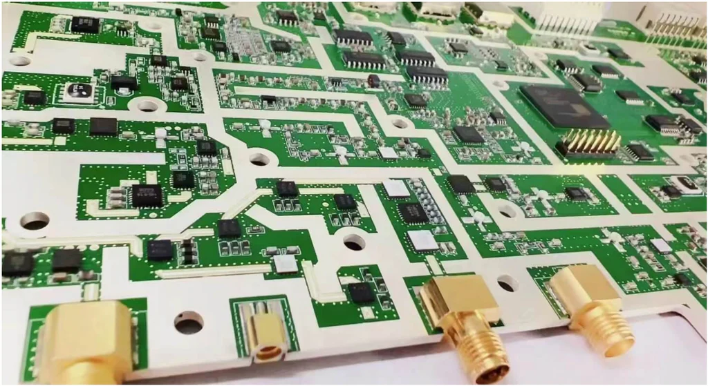
If you're designing a printed circuit board (PCB) for surface mount technology (SMT) assembly, one key factor you need to get right is SMD trace-to-pad spacing. So, what is the ideal spacing, and why does it matter? In short, SMD trace-to-pad spacing refers to the distance between a trace and the pad of a surface mount device (SMD). Proper spacing prevents issues like solder bridging, electrical shorts, and assembly errors during reflow soldering. A common guideline is to maintain at least 0.2 mm (8 mils) between traces and pads for standard designs, though this can vary based on your PCB manufacturing capabilities and design rules.
In this comprehensive guide, we'll dive deep into the importance of SMD trace spacing, provide actionable SMT assembly guidelines, and explore best practices for reflow soldering and solder paste application. Whether you're an engineer or a hobbyist, this blog will equip you with the knowledge to optimize your PCB designs for reliability and manufacturability.
Why SMD Trace-to-Pad Spacing Matters in SMT Assembly
When designing a PCB for SMT assembly, every detail counts. SMD trace-to-pad spacing is critical because it directly impacts the quality of soldering, the risk of defects, and the overall performance of your board. If the spacing is too tight, you risk solder bridging—where solder unintentionally connects adjacent pads or traces, causing a short circuit. If it's too wide, you may waste valuable board space, making your design less compact.
Proper spacing also ensures that automated pick-and-place machines and reflow soldering processes can work without errors. For instance, during reflow soldering, the solder paste must melt and form a strong bond between the component and the pad without spilling over to nearby traces. A well-planned spacing helps achieve this by giving enough room for solder to settle correctly.
Key Guidelines for SMD Trace Spacing
Determining the right trace-to-pad spacing depends on several factors, including the type of components, the manufacturing process, and the design rules provided by your PCB fabricator. Here are some practical guidelines to follow:
1. Follow Minimum Design Rules
Most PCB manufacturers provide design rule checks (DRC) that specify the minimum allowable spacing between traces and pads. A typical minimum spacing for standard designs is 0.2 mm (8 mils). For high-density designs, this might be reduced to 0.15 mm (6 mils), but only if your manufacturer supports finer tolerances. Always consult your fabricator's guidelines to avoid manufacturing issues.
2. Consider Component Size and Pad Geometry
Smaller components, like 0402 or 0201 resistors and capacitors, require tighter spacing due to their compact footprints. For example, an 0402 component might have pads spaced as close as 0.5 mm apart, meaning trace-to-pad spacing must be carefully calculated to avoid interference. Larger components, such as SOIC packages, allow for more generous spacing, often around 0.3 mm (12 mils) or more.
3. Account for Solder Mask and Stencil Design
Solder mask clearance around pads also affects trace-to-pad spacing. A typical solder mask clearance is 0.1 mm (4 mils) larger than the pad size. If traces are too close to the pad, the solder mask might not provide enough insulation, increasing the risk of shorts. Additionally, during solder paste application, the stencil openings must align precisely with the pads. Tight spacing can lead to paste misapplication, causing defects like insufficient solder or bridging.
SMT Assembly Guidelines for Flawless Results
Beyond trace-to-pad spacing, successful SMT assembly requires attention to several other design and process factors. These guidelines will help ensure your PCB is ready for manufacturing and performs reliably after assembly.
1. Optimize Component Placement
Place components in a way that minimizes trace lengths and avoids overcrowding. Group similar components together to streamline the pick-and-place process. For example, keep all 0402 resistors in one area of the board to reduce machine setup time. Also, ensure components are oriented consistently (e.g., all ICs facing the same direction) to simplify assembly and reduce errors.
2. Design for Thermal Balance During Reflow Soldering
During reflow soldering, uneven heating can cause issues like tombstoning, where one end of a component lifts off the pad. To prevent this, ensure that pads on either side of a component are of similar size and connected to similar copper areas. This balances the thermal mass and ensures even solder melting. For instance, if one pad of a 0603 resistor connects to a large ground plane while the other connects to a thin trace, the uneven heat distribution might cause tombstoning.
3. Adhere to IPC Standards
The Institute of Printed Circuits (IPC) provides widely accepted standards for PCB design and assembly. According to IPC-7351, a standard for surface mount design, trace-to-pad spacing should account for manufacturing tolerances and ensure at least 0.2 mm clearance for most designs. Following these standards reduces the risk of defects and ensures compatibility with most SMT assembly processes.
Reflow Soldering: Best Practices for SMD Assembly
Reflow soldering is the most common method for attaching SMD components to a PCB. It involves applying solder paste to the pads, placing components, and then heating the board in a reflow oven to melt the solder and form strong connections. Here’s how to optimize this process with proper design and preparation.
1. Use the Right Reflow Profile
A reflow profile defines the temperature and time settings in the reflow oven. A typical profile includes four stages: preheat, soak, reflow, and cooling. For lead-free solder, the peak temperature during reflow often reaches 245°C to 260°C for about 20-40 seconds, depending on the solder paste specifications. Ensure your PCB materials can withstand these temperatures—standard FR-4 material is usually rated for up to 260°C.
2. Avoid Overheating Sensitive Components
Some components, like certain LEDs or sensors, are sensitive to high temperatures. Check the datasheet for maximum temperature ratings and adjust your reflow profile if needed. If a component can only handle 235°C, for example, ensure the reflow peak stays below this threshold or consider hand soldering for that part after the main reflow process.
3. Inspect Post-Reflow Results
After reflow soldering, inspect the board for common issues like solder bridging, insufficient solder, or misaligned components. Automated optical inspection (AOI) systems can detect these defects with high accuracy. If bridges are found near traces, it might indicate that your trace-to-pad spacing is too tight, and adjustments are needed in future designs.
Solder Paste Application: Tips for Precision
Solder paste application is a critical step in SMT assembly, as it directly affects the quality of the solder joints formed during reflow. Here are some best practices to ensure precision and consistency.
1. Choose the Right Solder Paste
Solder paste consists of tiny solder alloy particles mixed with flux. For most SMT applications, a lead-free paste with a Type 3 or Type 4 particle size (20-38 microns for Type 3) is ideal. Smaller particle sizes, like Type 5, are better for ultra-fine pitch components but can be more expensive and harder to handle.
2. Design Stencils for Accuracy
The stencil used to apply solder paste must match the pad layout precisely. Stencil thickness typically ranges from 0.1 mm to 0.15 mm (4-6 mils) for standard designs. For fine-pitch components, reduce the stencil aperture by 10-20% compared to the pad size to prevent excess paste, which can lead to bridging. For example, if a pad is 0.6 mm wide, the stencil opening might be 0.5 mm to control paste volume.
3. Use Solder Paste Inspection (SPI)
Solder paste inspection (SPI) systems measure the height, area, and alignment of paste deposits after application. This step is crucial for detecting issues like insufficient paste or misalignment before components are placed. SPI can help catch problems early, especially in high-density designs where trace-to-pad spacing is minimal.
Common Challenges and How to Overcome Them
Even with careful planning, challenges can arise during SMT assembly. Here are some common issues related to SMD trace spacing and soldering, along with solutions.
1. Solder Bridging
If traces are too close to pads, solder can flow between them during reflow, creating a bridge. To fix this, increase the trace-to-pad spacing to at least 0.2 mm and ensure proper solder mask coverage. If bridging persists, consider reducing the stencil aperture to apply less paste.
2. Insufficient Solder Joints
If pads don’t receive enough solder paste, the resulting joints may be weak or incomplete. This can happen if the stencil is misaligned or if spacing issues cause paste to spread unevenly. Use SPI to verify paste volume and adjust stencil design if needed.
3. Component Misalignment
Tight trace-to-pad spacing can sometimes interfere with component placement, especially for automated assembly. Ensure there’s enough clearance around pads for the pick-and-place machine’s tolerances, typically at least 0.3 mm of free space around small components.
Final Thoughts on SMD Trace-to-Pad Spacing for SMT Assembly
Mastering SMD trace-to-pad spacing is essential for successful SMT assembly. By maintaining proper spacing—often starting at 0.2 mm (8 mils)—and following SMT assembly guidelines, you can minimize defects like solder bridging and tombstoning. Pay close attention to reflow soldering profiles and solder paste application techniques to ensure strong, reliable connections. With these practices in place, your PCB designs will not only meet manufacturing standards but also perform consistently in real-world applications.
Designing for manufacturability doesn’t have to be complex. Start with these actionable tips, adhere to industry standards like IPC-7351, and always collaborate with your PCB fabricator to align your design with their capabilities. By focusing on precision in trace spacing and assembly processes, you’ll achieve high-quality results every time.
 ALLPCB


