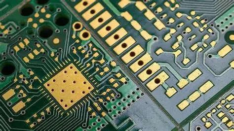
If you're a hobbyist diving into the world of printed circuit boards (PCBs), you might be wondering how to make sense of all those tiny components and markings. That’s where PCB silkscreen comes in—a layer of printed text and symbols on the board that helps with component identification and assembly. In this guide, we’ll walk you through the essentials of DIY PCB silkscreen, home etching techniques, silkscreen alternatives for hobbyists, component identification tips, and PCB assembly for beginners. Whether you're crafting a board at home or ordering a professional one, this post will help you navigate the process with ease.
What Is PCB Silkscreen and Why Does It Matter?
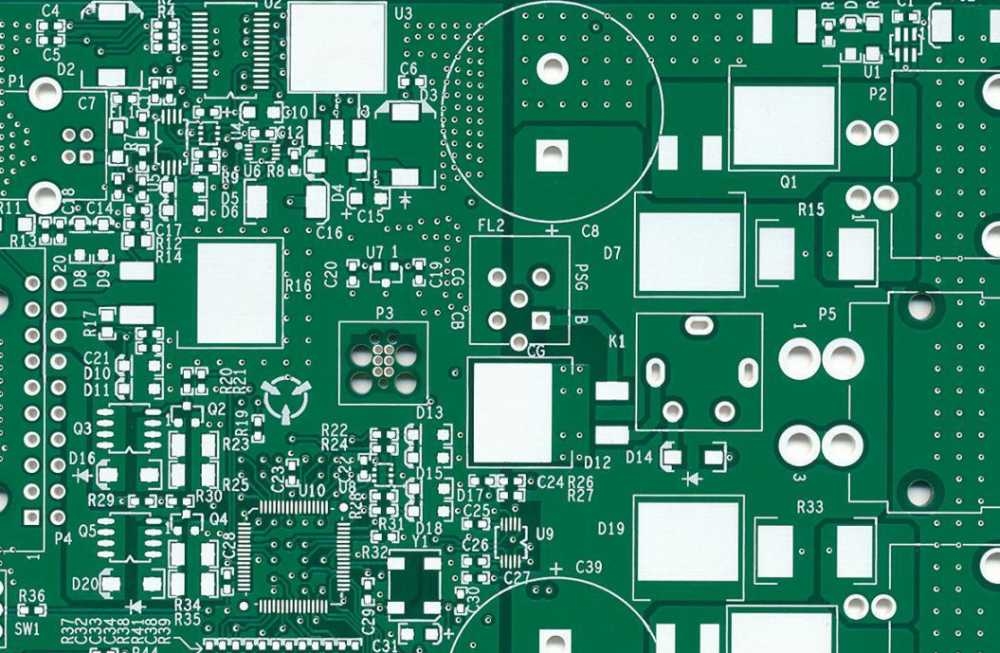
PCB silkscreen, often called the "legend," is the topmost layer of a PCB that contains printed text, symbols, and markings. These markings include reference designators (like R1 for a resistor), polarity indicators (for diodes or capacitors), and sometimes logos or version numbers. Typically made from a non-conductive epoxy ink, the silkscreen is applied in colors like white or black for visibility against the board’s surface.
For hobbyists, the silkscreen is a lifesaver. It simplifies component identification, reduces assembly errors, and ensures you place parts correctly during soldering. Without clear markings, assembling a PCB can feel like solving a puzzle with missing pieces—especially when dealing with dozens of tiny components.
Getting Started with DIY PCB Silkscreen at Home
Creating a silkscreen layer at home is entirely possible for hobbyists, even with limited tools. While professional manufacturers use advanced printing methods, you can achieve decent results with DIY techniques. Below, we’ll explore a simple method for DIY PCB silkscreen that’s both affordable and effective.
Materials You’ll Need for DIY Silkscreen
- A PCB (etched and drilled, ready for markings).
- Glossy photo paper or transparency film for printing your design.
- A laser printer to create a mirrored silkscreen design.
- An iron or heat press for toner transfer.
- Acetone or rubbing alcohol for cleanup (optional).
- White or colored paint pens for manual touch-ups (if needed).
Step-by-Step Guide to DIY PCB Silkscreen
- Design Your Silkscreen: Use PCB design software to create your silkscreen layer. Include reference designators, polarity markers, and any custom text. Ensure the design is mirrored since it will be transferred onto the board.
- Print the Design: Print the mirrored design onto glossy photo paper or transparency film using a laser printer. The toner acts as the transfer medium.
- Transfer the Toner: Place the printed design face-down on your PCB. Use an iron set to medium heat (around 150-180°C or 300-350°F) to press the design onto the board for 2-3 minutes. Apply even pressure to ensure the toner sticks properly.
- Peel and Clean: Let the board cool, then gently peel off the paper. If any toner didn’t transfer, you can touch it up with a permanent marker or paint pen. Optionally, clean excess residue with acetone.
- Seal the Silkscreen (Optional): For durability, apply a thin layer of clear varnish or epoxy over the silkscreen to protect it from scratches during handling.
This method is ideal for hobbyists because it uses common household items and doesn’t require expensive equipment. However, keep in mind that DIY silkscreen may not be as precise as professional printing, especially for very small text (below 6-point font size).
Home Etching Silkscreen: Challenges and Tips
If you’re etching your PCB at home, adding a silkscreen layer can be tricky since etching focuses on copper traces rather than surface markings. However, you can integrate silkscreen into your workflow by applying it after etching and drilling. Here are some challenges and tips for home etching silkscreen:
- Challenge - Surface Damage: Etching chemicals like ferric chloride can damage or corrode silkscreen markings if applied beforehand. Always add silkscreen after etching.
- Tip - Timing: Complete all copper etching and drilling before attempting silkscreen transfer. This prevents misalignment or damage to your markings.
- Challenge - Precision: Hand-aligning silkscreen designs on a home-etched board can lead to errors, especially on double-sided PCBs.
- Tip - Use Guides: Print alignment markers on your silkscreen design to match with drilled holes or board edges for better accuracy.
Home etching is a fantastic skill for hobbyists, but it requires patience. If silkscreen alignment feels too difficult, consider practicing on scrap boards before working on your final project.
Silkscreen Alternatives for Hobbyists
Not everyone has the time or tools for DIY silkscreen, and that’s okay. There are several silkscreen alternatives for hobbyists that can still help with component identification and assembly. Here are a few practical options:
1. Manual Labeling with Markers
Use a fine-tip permanent marker or paint pen to manually label components on your PCB. While this isn’t as neat as a printed silkscreen, it’s quick and effective for small projects. White or silver markers work best on dark PCB surfaces.
2. Stickers or Decals
Print your labels on sticker paper or transparency film, cut them out, and stick them onto the PCB. This method is great for temporary markings or prototypes since stickers can peel off over time.
3. Engraving or Scratching
If you have a small engraving tool or even a sharp object, you can lightly scratch reference designators into the PCB surface. This is a permanent solution but requires a steady hand and isn’t suitable for complex designs.
4. Professional Silkscreen Services
For a polished look without the hassle, consider ordering PCBs with silkscreen from a manufacturing service. Many providers offer affordable options for small batches, saving you time while ensuring precision.
Each of these alternatives has its pros and cons, so choose based on your project needs, budget, and skill level. For most beginners, starting with manual labeling is the easiest way to get comfortable with component identification.
Component Identification Tips for Beginners
Understanding how to read and use silkscreen markings is just as important as creating them. Here are some component identification tips to help you assemble PCBs with confidence:
1. Learn Reference Designators
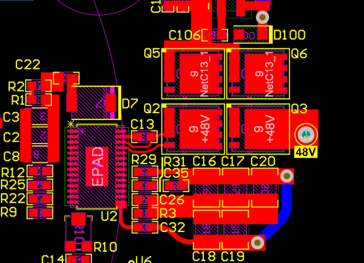
Reference designators are codes printed on the silkscreen to identify components. Common ones include:
- R for resistors (e.g., R1, R2).
- C for capacitors (e.g., C1, C2).
- D for diodes (e.g., D1).
- Q for transistors (e.g., Q1).
- U for integrated circuits (e.g., U1).
Matching these codes with a schematic or bill of materials (BOM) tells you exactly which part goes where.
2. Check Polarity Markings
Components like diodes, capacitors, and LEDs have polarity, meaning they must be placed in the correct orientation. Look for silkscreen symbols like a “+” sign, a stripe, or an arrow to guide you. Incorrect polarity can damage components or prevent the circuit from working.
3. Use a Magnifying Glass or Loupe
PCB markings can be tiny, especially on compact boards. A magnifying glass or jeweler’s loupe (with 5x to 10x magnification) can help you read small text and symbols clearly.
4. Cross-Reference with Documentation
Always keep your schematic and BOM handy during assembly. These documents provide detailed information about component values (e.g., a 10kΩ resistor or a 100uF capacitor) that might not fit on the silkscreen due to space constraints.
5. Test Continuity for Confirmation
After placing components, use a multimeter to test continuity between pads and ensure they match the silkscreen markings. This can catch errors before powering up the board.
By mastering these tips, you’ll reduce mistakes and build PCBs more efficiently, even as a beginner.
PCB Assembly for Beginners: Best Practices
Once you’ve got your silkscreen or alternative markings in place, it’s time to assemble your PCB. PCB assembly for beginners can seem daunting, but following these best practices will make the process smoother:
1. Organize Your Components
Before soldering, sort your components by type and value. Use small containers or a component tray to keep resistors, capacitors, and ICs separate. Label them if needed to avoid confusion.
2. Start with Low-Profile Components
Solder smaller, low-profile components like resistors and diodes first. This keeps the board flat and makes it easier to access pads for taller components like capacitors or connectors later.
3. Double-Check Placement
Refer to your silkscreen markings and schematic to confirm each component’s position and orientation before soldering. It’s much harder to desolder a misplaced part than to check twice.
4. Use the Right Tools
Invest in a good soldering iron with a fine tip (around 25-30 watts for hobbyist work) and use lead-free solder with a diameter of 0.5-0.8mm for precision. A pair of tweezers is also handy for handling small parts.
5. Test as You Go
After soldering a section of the board, test for shorts or open circuits with a multimeter. This helps catch issues early, especially in complex designs with multiple power rails (e.g., 3.3V and 5V lines).
Assembly takes practice, so don’t worry if your first board isn’t perfect. Over time, you’ll develop a steady hand and a keen eye for detail.
Common Mistakes to Avoid with PCB Silkscreen and Assembly
Even with the best intentions, hobbyists often make mistakes when working with silkscreen and PCB assembly. Here are some pitfalls to watch out for:
- Overloading the Silkscreen: Too much text or cluttered markings can make the board hard to read. Stick to essential information like reference designators and polarity indicators.
- Ignoring Font Size: Text smaller than 6 points (or 0.8mm in height) may not transfer well in DIY methods or be legible. Test your design on paper first.
- Misaligning Markings: If your silkscreen doesn’t match the component footprints, it can lead to assembly errors. Always double-check alignment during design and transfer.
- Soldering Without Verification: Rushing to solder without confirming component placement often results in rework. Take your time to verify each part.
Avoiding these mistakes will save you time and frustration, especially on your first few projects.
Conclusion: Mastering Silkscreen and Component Identification as a Hobbyist
As a hobbyist, learning the ins and outs of PCB silkscreen and component identification is a game-changer. Whether you’re using DIY PCB silkscreen techniques, exploring home etching silkscreen methods, or opting for silkscreen alternatives, the goal is to make your assembly process smoother and more accurate. By following the component identification tips and PCB assembly best practices outlined in this guide, you’ll build confidence in creating functional, well-organized boards.
Start small, experiment with different methods, and don’t be afraid to make mistakes—they’re part of the learning curve. With practice, you’ll master the art of silkscreen and assembly, turning your ideas into working circuits. Keep this guide handy as you embark on your next project, and enjoy the rewarding journey of PCB design and creation!
 ALLPCB


