ALLPCB


Introduction
The bipolar transistor is one of the fundamental semiconductor components, providing current amplification and serving as a core element in electronic circuits. As a discrete active semiconductor device, transistors come in many forms. In the narrow sense, "transistor" refers to bipolar junction transistors (BJTs), which are the most basic and common type. This article focuses on silicon NPN bipolar transistors.
History
Before the advent of crystal transistors, vacuum tube triodes were used for amplification and switching in electronic circuits. Vacuum tubes were bulky, power-hungry, and slow. During World War II there was an urgent military need for a stable, reliable, and fast signal amplifier, and research after the war led to the transistor. Early devices used germanium because it was easier to obtain; with the development of silicon and efficient silicon processing, germanium devices were gradually phased out.
Basic Structure of a BJT
The core of a bipolar transistor is two back-to-back PN junctions. These can form either an NPN or a PNP structure. Since silicon NPN transistors are the mainstream today, the following description uses the silicon NPN as the example.
Device Structure and Process Characteristics
Typical structural and process characteristics of a silicon NPN transistor include:
- Heavily doped emitter: The emitter is doped more heavily than the base to facilitate electron emission; the emitter junction area is relatively small.
- Thin base region: The base thickness is thin, typically 3–30 μm, with a relatively low doping concentration.
- Large collector area: The collector is of the same conductivity type as the emitter but is more lightly doped and has a large area to efficiently collect carriers.
A transistor is not simply the sum of two diodes. The relative materials, dimensions, layout, doping concentrations, and geometry of the PN junctions determine device behavior and enable many types of semiconductor components, including integrated circuits.
Symbol and Current-Control Principle
In typical operation the emitter-base junction is forward biased and the collector-base junction is reverse biased.
Current relationships:
IE = IB + IC
IC = β × IB
If IB = 0, then IE = IC = 0.
Characteristic Curves
Input characteristic: For a given collector-emitter voltage UCE, the input characteristic shows the relationship between base current IB and base-emitter voltage UBE.
Output characteristic: For fixed base current IB, the output characteristic shows the relationship between collector current IC and collector-emitter voltage UCE; a family of curves is obtained for different IB values.
- When IB = 0, IC ≈ 0: the transistor is in cutoff, equivalent to an open switch.
- When IB > 0, small changes in IB can produce IC changes amplified by tens to hundreds of times.
- When IB becomes large enough, IC saturates and no longer increases proportionally with IB; the transistor loses its amplification action and behaves like a closed switch.
Core Functions
- Amplification: Small changes in input current produce larger changes in output current.
- Switching: A small control current can switch a larger current on or off.
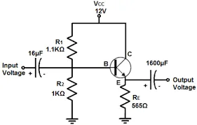
Amplification Example
IC = β × IB, where β is typically in the range 10–400.
Example: For IB = 50 μA and β = 120, IC = 120 × 50 μA = 6000 μA. A small signal current can therefore be amplified into a much larger current signal. Note that a transistor amplifies signal amplitude; it does not create energy.
Main Performance Parameters
Transistor parameters are categorized as DC, AC, and limit parameters.
| Category | Parameter | Symbol | Meaning |
|---|---|---|---|
| DC | Common-emitter DC current gain | β | Ratio of collector current to base current with no alternating signal, β = IC / IB |
| Common-base DC current gain | α | Ratio of collector current to emitter current with no alternating signal | |
| Collector-emitter leakage current | ICEO | Reverse collector-emitter current with base open, also called leakage or saturation current | |
| Collector-base leakage current | ICBO | Collector-base reverse current with emitter open; ICEO = β × ICBO | |
| AC | Common-emitter AC current gain | β | Ratio of incremental collector current to incremental base current: β = ΔIC / ΔIB |
| Common-base AC current gain | α | Ratio of incremental collector current to incremental emitter current: α = ΔIC / ΔIE | |
| Common-emitter cutoff frequency | fβ | Frequency at which β drops by 3 dB | |
| Common-base cutoff frequency | fα | Frequency at which α drops by 3 dB | |
| Transition frequency | fT | Frequency at which β falls to 1 | |
| Limits | Maximum collector current | ICM | Maximum allowable collector current |
| Maximum collector power | PCM | Exceeding this power will damage the transistor | |
| Collector-emitter breakdown voltage | UCEO | Collector-emitter voltage withstand with base open |
Temperature Effects
Temperature affects nearly all transistor parameters. The three most affected parameters are:
- Gain β: For a fixed base current IB, collector current IC can increase rapidly with temperature.
- Reverse saturation current (leakage) ICEO: Formed by minority carrier drift; ICEO increases rapidly with temperature—approximately doubling for every 10 °C rise.
- Emitter-base voltage UBE: UBE decreases by about 2.2 mV per 1 °C rise.
As temperature rises, β and IC increase while UCE decreases. Circuit design should account for these effects through thermal management such as heat sinking and placement away from heat sources.
Classification
Transistors are classified from multiple perspectives.
| Perspective | Type | Remarks |
|---|---|---|
| Materials | By semiconductor | Silicon transistor VBE ≈ 0.6 V; germanium transistor VBE ≈ 0.3 V |
| By structure | PNP, NPN | |
| By manufacturing | Planar, alloy, diffusion | |
| Performance | By frequency | Low frequency: < 3 MHz; Medium: 3–30 MHz; High: 30–500 MHz; Ultra-high: > 500 MHz |
| By power | Small power: PCM < 0.5 W; Medium: ~0.5–1 W; Large power: PCM > 1 W | |
| By function | Amplifier, switch, high-voltage, phototransistor, digital switching | |
| By package | By material and form | |
| By package style | Through-hole: TO series; Surface-mount: SOT series |
Naming Conventions
Different regions and manufacturers use different naming systems; manufacturers may also adopt proprietary schemes.
Transistor naming in China
| 3 | D | D | 12 | X |
|---|---|---|---|---|
| 2: diode; 3: transistor | A: PNP germanium; B: NPN germanium; C: PNP silicon; D: NPN silicon | X: low-frequency small power; G: high-frequency small power; D: low-frequency high-power; A: high-frequency high-power | Sequence number | Specification number |
Example: 3DD12X indicates an NPN, low-frequency, high-power silicon transistor.
Japanese naming
| 2 | S | D | 13 | B |
|---|---|---|---|---|
| 0: phototransistor; 1: diode; 2: transistor | Registered prefix | A: PNP high frequency; B: PNP low frequency; C: NPN high frequency; D: NPN low frequency | Registration sequence | Variant |
Example: 2SC1895 is an NPN high-frequency transistor.
U.S. (EIA) naming
| JANS | 2 | N | 2904 | A |
|---|---|---|---|---|
| JANTX: special military; JANTXV: extended military; JANS: aerospace; (none): commercial | 1: diode; 2: transistor; "n": n junction devices | EIA registered identifier | EIA sequence number | Variant grade |
Example: JANS2N2904 is an aerospace-grade transistor.
European naming
| B | C | 208 | A |
|---|---|---|---|
| A: germanium; B: silicon | C: low-frequency small power; D: low-frequency large power; F: high-frequency small power; L: high-frequency large power | Registration sequence | β category |
Example: BC208A is a silicon, low-frequency, small-power transistor.
Packaging and Pin Assignment
Packaging
Larger rated power requires larger packages; packaging technology has evolved, so many package forms exist. Plastic packages are currently the mainstream, with TO and SOT styles common.
Pin assignment
Pin assignments vary by manufacturer and package. General rules include:
- For medium and high-power transistors, the collector is often a large metal tab or heatsink connection and is typically between the base and emitter physically.
- For surface-mount transistors, when viewing the marking, the left pin is often the base, the right pin the emitter, and the collector is on the opposite side.
Base — B; Collector — C; Emitter — E.
Selection Guidelines
When selecting a transistor, respect device limits and apply a 2/3 safety margin for critical parameters.
- Collector current IC: IC < 2/3 × ICM, where ICM is the maximum allowable collector current. If IC > ICM, β decreases and the device may lose amplification function.
- Collector power PW: PW < 2/3 × PCM, where PCM is the maximum allowable power. Exceeding PCM can destroy the transistor.
- Collector-emitter reverse voltage UCE: UCE < 2/3 × UBVCEO, where UBVCEO is the breakdown voltage with base open. If UCE > UBVCEO, destructive breakdown can occur.
- Operating frequency: Use up to about 15% of fT (transition frequency) for reliable amplification. As frequency increases, gain decreases, and at fT the gain is approximately 1.
Also consider size and cost; surface-mount packages are often preferred for compact designs.