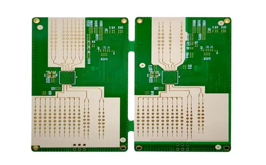
In the fast-paced world of electronics, creating smaller, faster, and more efficient printed circuit boards (PCBs) is a constant challenge. One groundbreaking solution that’s transforming the industry is the use of embedded capacitors in PCB design. But what exactly are embedded capacitors, and how do they contribute to PCB miniaturization techniques? Simply put, embedded capacitors are integrated directly into the PCB layers, eliminating the need for surface-mounted components and saving valuable space while enhancing performance, especially in high-frequency applications. In this blog, we’ll dive deep into the benefits of embedded capacitor PCB design, explore techniques for miniaturization, and provide actionable insights for optimizing your designs.
What Are Embedded Capacitors and Why Do They Matter?
Embedded capacitors are capacitive elements built directly into the internal layers of a PCB, rather than being placed on the surface as discrete components. They are formed by sandwiching a thin dielectric material between two conductive layers, creating capacitance without taking up surface real estate. This innovation is a game-changer for engineers working on compact, high-performance devices.
Why do they matter? In modern electronics, space is at a premium. Devices like smartphones, wearables, and IoT gadgets demand smaller PCBs without sacrificing functionality. Embedded capacitors address this by reducing the number of surface components, which not only aids PCB miniaturization techniques but also improves signal integrity and power delivery in high-frequency PCB design. For instance, they help maintain a stable power supply by acting as decoupling capacitors, reducing noise in circuits operating at frequencies above 1 GHz.
The Role of Embedded Capacitors in PCB Miniaturization Techniques
Miniaturization is the driving force behind many technological advancements. As devices shrink, so must the components and boards that power them. Embedded capacitor PCB design plays a pivotal role in this by freeing up surface space and allowing for denser layouts. Let’s explore how this works.
First, by embedding capacitors within the PCB substrate, designers can eliminate the need for numerous surface-mounted decoupling capacitors. A typical high-speed design might require dozens of 0.1 μF capacitors for power integrity. Embedding these capacitors can reduce the component count by up to 50%, according to industry studies, leaving more room for other critical elements.
Second, embedded capacitors enable thinner PCB stackups. Traditional designs often require additional layers to accommodate surface components, increasing the board’s thickness. With embedded solutions, you can achieve the same capacitance in a slimmer profile, which is crucial for ultra-thin devices like smartwatches.
Finally, this approach supports the trend toward smaller form factors in industries like automotive and medical electronics. For example, embedded capacitors are ideal for compact sensor modules where every square millimeter counts.
Enhancing High-Frequency PCB Design with Embedded Capacitors
High-frequency PCB design is a critical area where embedded capacitors shine. As signal speeds increase—often exceeding 5 GHz in applications like 5G communication—maintaining power integrity and minimizing noise become paramount. Embedded capacitors offer unique advantages in these scenarios.
One major benefit is their ability to reduce parasitic inductance. In traditional designs, surface-mounted capacitors have longer traces connecting them to the power and ground planes, introducing inductance that can degrade performance at high frequencies. Embedded capacitors, placed directly within the PCB layers, shorten these paths, minimizing parasitic inductance in PCB layouts to as low as 0.1 nH in some cases.
Additionally, embedded capacitors provide better decoupling at high frequencies. They can respond to rapid voltage fluctuations faster than surface components, ensuring a stable power delivery network (PDN). This is especially important for RF circuits and high-speed digital systems where even a small voltage spike can cause signal distortion.
For practical implementation, designers should focus on selecting dielectric materials with high capacitance density and low loss tangent for embedded layers. Materials with a dielectric constant (Dk) above 10 are often recommended for high-frequency applications to achieve sufficient capacitance in a small area.
Optimizing Decoupling Capacitor Placement with Embedded Technology
Decoupling capacitor placement is a critical aspect of PCB design, especially for maintaining power integrity. The goal is to position capacitors as close as possible to the power pins of integrated circuits (ICs) to filter out noise and stabilize voltage. Embedded capacitors take this concept to the next level.
Unlike surface-mounted capacitors, which are limited by physical space and trace length, embedded capacitors can be integrated directly beneath the ICs within the PCB stackup. This proximity reduces the loop inductance and enhances the decoupling effect. For instance, in a design with a high-speed processor operating at 3.2 GHz, embedding a 1 nF capacitor directly under the IC can reduce voltage ripple by up to 30% compared to a surface-mounted solution.
To optimize placement, designers should use simulation tools to analyze the PDN impedance across a range of frequencies (from kHz to GHz). This helps identify the ideal locations for embedded capacitance to suppress noise effectively. Additionally, combining embedded capacitors with a few strategically placed surface capacitors can address both low- and high-frequency noise, creating a balanced design.
Minimizing Parasitic Inductance in PCB Layouts
Parasitic inductance is the enemy of high-speed and high-frequency designs. It can cause voltage drops, signal delays, and electromagnetic interference (EMI). Minimizing parasitic inductance in PCB layouts is therefore a top priority, and embedded capacitors offer a powerful solution.
The key advantage of embedded capacitors is their integration into the PCB’s internal layers, which shortens the distance between the capacitor and the power/ground planes. In a typical surface-mounted design, the trace length might introduce an inductance of 1-2 nH. With embedded capacitors, this can be reduced to below 0.2 nH, significantly improving performance.
To further minimize inductance, designers should ensure tight coupling between power and ground planes in the PCB stackup. Using thin dielectric layers (e.g., 0.1 mm or less) between these planes can create additional planar capacitance, complementing the embedded capacitors. Additionally, avoid unnecessary vias in the power delivery path, as each via can add 0.5-1 nH of inductance.
For high-frequency designs, it’s also worth considering the self-resonant frequency (SRF) of embedded capacitors. Choose materials and configurations that push the SRF beyond the operating frequency of your circuit to avoid resonance issues. For example, an embedded capacitor with an SRF of 2 GHz is suitable for applications up to 1.5 GHz.
Challenges and Considerations in Embedded Capacitor PCB Design
While embedded capacitors offer incredible benefits, they come with challenges that designers must address. Understanding these hurdles ensures a successful implementation in your projects.
One challenge is the limited capacitance range. Embedded capacitors typically provide lower capacitance values (in the range of pF to nF) compared to surface-mounted components, which can offer μF values. This means they may not fully replace larger decoupling capacitors in designs requiring high capacitance.
Another consideration is the cost. Manufacturing PCBs with embedded capacitance often involves specialized materials and processes, which can increase production expenses. However, the cost is often justified by the space savings and performance gains, especially in high-end applications.
Lastly, design complexity can be a barrier. Creating an effective embedded capacitor layout requires precise control over layer thickness, dielectric properties, and stackup configuration. Partnering with a reliable PCB manufacturer with expertise in advanced designs can help overcome this challenge.
Practical Tips for Implementing Embedded Capacitors
Ready to integrate embedded capacitors into your next project? Here are some practical tips to get started with embedded capacitor PCB design:
- Choose the Right Material: Select dielectric materials with high capacitance density and compatibility with standard PCB fabrication processes. Look for materials with a dielectric constant above 10 for high-frequency applications.
- Simulate Early: Use simulation software to model the PDN and predict the impact of embedded capacitors on impedance and noise. This helps fine-tune the design before manufacturing.
- Balance with Surface Components: Combine embedded capacitors with a few surface-mounted ones to cover a wide frequency range. For example, use embedded capacitors for high-frequency noise and surface capacitors for low-frequency bulk decoupling.
- Optimize Stackup: Design your PCB stackup to place embedded capacitor layers close to high-speed ICs, minimizing loop inductance and maximizing decoupling efficiency.
- Test Thoroughly: After fabrication, test the board’s power integrity and signal performance to validate the effectiveness of the embedded capacitors.
Future Trends: Embedded Capacitors and Beyond
The adoption of embedded capacitors is just the beginning of a broader trend toward fully integrated PCB solutions. As technology evolves, we’re likely to see even more components—such as resistors and inductors—embedded within PCB substrates. This will further drive PCB miniaturization techniques, enabling the creation of incredibly compact and efficient devices.
In high-frequency PCB design, advancements in dielectric materials will push the boundaries of what’s possible with embedded capacitors. Researchers are developing materials with ultra-high dielectric constants (above 50) and minimal loss, which could revolutionize power delivery in 6G networks and beyond.
Additionally, the rise of automated design tools and artificial intelligence will simplify the integration of embedded components. These tools can optimize decoupling capacitor placement and predict parasitic effects with unprecedented accuracy, making advanced designs accessible to more engineers.
Conclusion: Embrace the Power of Embedded Capacitors
Embedded capacitors are revolutionizing PCB design by enabling unprecedented levels of miniaturization and performance. From supporting PCB miniaturization techniques to enhancing high-frequency PCB design, they offer a powerful way to meet the demands of modern electronics. By minimizing parasitic inductance in PCB layouts and optimizing decoupling capacitor placement, embedded capacitors help engineers create smaller, faster, and more reliable boards.
While challenges like cost and design complexity exist, the benefits far outweigh the drawbacks for many applications. Whether you’re working on a compact IoT device or a high-speed communication system, consider leveraging embedded capacitor PCB design to take your project to the next level. With the right materials, tools, and manufacturing support, you can unlock the full potential of this innovative technology.
 ALLPCB


