 ALLPCB


If you're looking to achieve flawless results in high-density PCB assembly, precision solder masking is a critical step. This process ensures protection of copper traces, prevents short circuits, and supports fine-pitch components in compact designs. In this comprehensive guide, we’ll dive into the techniques and best practices for solder mask application, focusing on solder mask high density assembly, fine pitch solder mask, solder mask alignment accuracy, and solder mask web optimization. Whether you're an engineer or a designer, you'll find actionable insights to enhance your PCB projects.
What Is Solder Masking and Why Does It Matter in High-Density PCB Assembly?
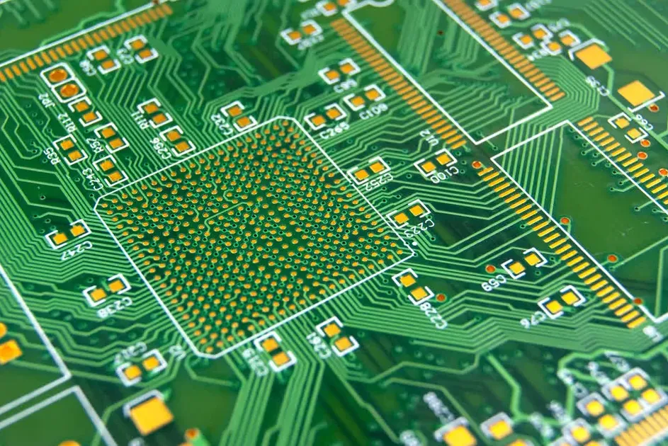
Solder masking, also known as solder resist, is the process of applying a thin protective layer over the copper traces of a printed circuit board (PCB). This layer serves multiple purposes: it shields the copper from oxidation, prevents solder bridges during assembly, and insulates conductive paths to avoid short circuits. In high-density PCB assembly, where components are packed tightly with minimal spacing, the role of solder masking becomes even more crucial. A precise solder mask ensures that fine-pitch components—those with lead spacings as small as 0.5 mm or less—can be soldered accurately without defects.
High-density designs often involve complex layouts with numerous traces and vias squeezed into a small area. Without a properly applied solder mask, the risk of electrical interference or soldering errors skyrockets. By optimizing the solder mask process, manufacturers can achieve higher reliability and performance in applications like smartphones, medical devices, and automotive electronics.
Key Benefits of Precision Solder Masking
- Protects copper traces from environmental damage and oxidation.
- Prevents solder bridges in fine-pitch soldering, reducing defects.
- Enhances insulation for high-density layouts, supporting trace widths as narrow as 3 mils (0.076 mm).
- Improves overall PCB durability and longevity.
Challenges in Solder Masking for High-Density PCB Assembly
Applying a solder mask to high-density PCBs is no easy task. The compact nature of these boards introduces unique challenges that require advanced techniques and meticulous attention to detail. Below are some common hurdles in solder mask high density assembly and how they impact the process.
1. Fine-Pitch Component Placement
Fine-pitch components, often with pin spacings below 0.65 mm, demand exceptional precision in solder mask application. Any misalignment or excess mask material can cover solder pads, leading to poor connections or soldering defects. For instance, a mask overlap of just 0.1 mm can disrupt the soldering process for components like quad flat no-lead (QFN) packages.
2. Narrow Trace and Via Clearances
In high-density designs, traces and vias are often spaced less than 0.1 mm apart. This tight spacing leaves little room for error in solder mask alignment. If the mask encroaches on these areas, it can interfere with electrical performance or cause shorts during assembly.
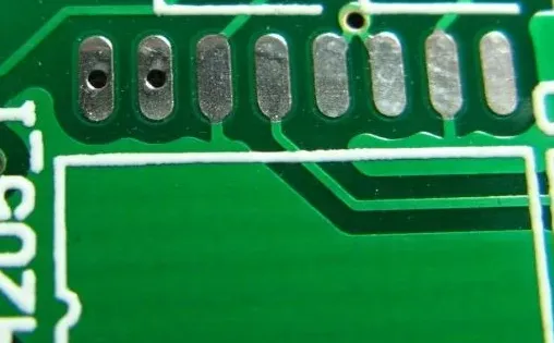
3. Solder Mask Web Optimization
The "web" refers to the thin strip of solder mask between pads or traces. In high-density boards, optimizing this web is critical to prevent mask peeling or cracking. A web thickness of less than 0.08 mm may be too fragile, while a thicker web might not fit within the design constraints.
Techniques for Precision Solder Masking in High-Density Assembly
To overcome the challenges of solder mask high density assembly, manufacturers rely on advanced techniques tailored to the unique needs of compact PCB designs. Here are some proven methods to ensure accuracy and reliability.
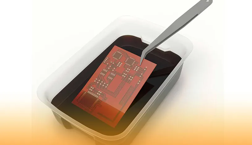
1. Liquid Photoimageable (LPI) Solder Mask Application
LPI solder masks are widely used in high-density PCB assembly due to their ability to achieve fine resolution. This method involves applying a liquid mask material that is then exposed to UV light through a photomask to define the pattern. LPI masks can achieve a resolution of up to 0.05 mm, making them ideal for fine-pitch solder mask applications. They also provide uniform coverage, reducing the risk of defects in tight spaces.
2. High-Resolution Imaging for Solder Mask Alignment Accuracy
Alignment accuracy is paramount in high-density designs. Modern manufacturing processes use high-resolution imaging systems to align the solder mask with the PCB layout. These systems can achieve alignment tolerances as tight as ±0.025 mm, ensuring that the mask does not overlap critical areas like solder pads or vias. This precision is especially important for boards with trace widths below 0.1 mm.
3. Controlled Curing Processes
After application, the solder mask must be cured to harden and adhere to the PCB surface. Controlled curing—using a combination of UV exposure and thermal baking—ensures that the mask maintains its integrity even in high-density areas. Over-curing can lead to brittleness, while under-curing may cause peeling. A typical curing process might involve UV exposure at 100 mJ/cm2 followed by baking at 150°C for 30 minutes.
4. Solder Mask Web Optimization for Durability
Optimizing the solder mask web involves balancing thickness and material properties to prevent cracking or peeling. For high-density boards, a web width of 0.1 mm to 0.15 mm is often ideal, providing enough strength without encroaching on adjacent features. Advanced materials with higher tensile strength can also improve web durability in tight spaces.
Best Practices for Solder Masking in High-Density PCB Assembly
Beyond specific techniques, adopting best practices can significantly improve the quality of solder masking in high-density PCB assembly. These guidelines focus on design, material selection, and process control to ensure consistent results.
1. Design for Manufacturability (DFM) in Solder Mask Layout
Start with a PCB layout that accounts for solder mask constraints. Ensure that solder mask openings are slightly larger than the solder pads—typically by 0.05 mm to 0.1 mm on each side—to accommodate alignment tolerances. Avoid placing vias too close to pads, as this increases the risk of mask encroachment. Following DFM guidelines can reduce manufacturing defects by up to 30%.
2. Choose the Right Solder Mask Material
Not all solder mask materials are suited for high-density applications. For fine-pitch designs, select a material with high dielectric strength (above 500 V/mil) and low viscosity for better flow into tight spaces. Green is the most common color due to its visibility and contrast, but other colors like black or blue may be used for specific aesthetic or functional requirements.
3. Maintain Tight Process Controls
Consistency is key in solder mask application. Monitor parameters like mask thickness (typically 0.02 mm to 0.03 mm after curing), curing temperature, and exposure time to avoid variations. Automated inspection systems can detect defects like pinholes or misalignment with an accuracy of 0.01 mm, ensuring quality in every batch.
4. Test for Reliability in High-Density Areas
After applying the solder mask, conduct thorough testing to verify its performance. Electrical testing can confirm insulation resistance, often targeting values above 10^12 ohms for high-density designs. Thermal cycling tests—exposing the board to temperature swings between -40°C and 125°C—can also reveal weaknesses in the mask adhesion or web structure.
Common Solder Mask Defects in High-Density Assembly and How to Avoid Them
Even with the best techniques, defects can occur during solder masking. Identifying and addressing these issues early can save time and cost in high-density PCB assembly. Here are some frequent problems and solutions.
1. Solder Mask Peeling or Delamination
Peeling often results from poor adhesion due to surface contamination or improper curing. Ensure the PCB surface is clean and free of residues before mask application. Use a curing process that matches the material specifications, such as baking at 150°C for 30-60 minutes.
2. Misalignment of Solder Mask Openings
Misalignment can block solder pads or expose unintended areas. Use high-precision alignment tools with tolerances below 0.03 mm, and double-check the photomask design against the PCB layout before processing.
3. Pinholes or Voids in the Solder Mask
Pinholes occur when air bubbles or debris interfere with mask application. Maintain a clean manufacturing environment and use vacuum-assisted coating methods to minimize trapped air. Inspect the mask under magnification to catch defects early.
Conclusion: Mastering Solder Masking for High-Density PCB Success
Precision solder masking is a cornerstone of successful high-density PCB assembly. By addressing challenges like fine-pitch component placement, narrow trace clearances, and solder mask web optimization, manufacturers can achieve reliable and high-performing boards. Techniques such as liquid photoimageable masking, high-resolution alignment, and controlled curing, combined with best practices in design and testing, ensure that the solder mask meets the demands of modern electronics.
Whether you're working on compact consumer devices or critical industrial systems, focusing on solder mask alignment accuracy and material selection can make all the difference. With the right approach, you can minimize defects, improve yield, and deliver PCBs that meet the highest standards of quality and performance.
At ALLPCB, we’re committed to supporting your high-density PCB projects with cutting-edge manufacturing solutions. Explore our services to see how we can help you achieve precision in every layer of your design.


