ALLPCB


Overview
In the off state, the body diode structure of a power MOSFET is designed to block the minimum drain-to-source voltage. Breakdown or avalanche of the body diode indicates that the electric field across the reverse-biased body diode has driven a large current between the drain and source terminals. Typical off-state leakage currents are on the order of tens of pA to hundreds of nA. Previously published material covered MOSFET avalanche effects; this article focuses on UIS/UIL ratings found in datasheets.
UIS Energy Ratings and SOA
Besides Ipk versus tav plots, most power MOSFET datasheets include a UIS energy rating, often listed in the absolute maximum table. This can be misleading because, in theory (E = 0.5 * Vav * Ipk * tav), a MOSFET could show arbitrarily large energy if measured with infinitesimally small inductance (tav → 0) or infinitely large inductance (tav → ∞). In practice, avalanche pulse energy absorbed by a MOSFET increases with tav. For a given initial junction temperature Tj(initial), any single UIS energy rating corresponds to a working point on the Ipk versus tav SOA curve.
Reasons for choosing one working point as the datasheet "maximum" include using the same point for production-line screening or indicating a particular energy level for customer information. When comparing UIS capability between devices, it is crucial to compare the Ipk versus tav curves at the same Tj(initial), rather than comparing single UIS energy numbers.
Thermal Limits and Scaling with Active Die Volume
Several design and wafer-processing attributes influence MOSFET UIS capability. The most significant is the design and processing of the source metal contacts. However, for understanding UIS behavior the key concept is thermal failure: the energy dissipated during avalanche is limited by the device thermal capability for that power function. MOSFETs with similar breakdown (BV) characteristics and similar thermal performance will exhibit similar UIS capability. Because typical UIS avalanche durations in practical applications are usually less than 1 ms, heat flow is not strongly affected by external thermal boundary conditions; the primary thermal constraints are the active die area and thickness of the bare die. Therefore, within a MOSFET technology, the Ipk(fail) versus tav capability is expected to scale with active die area. Figure 1 confirms this.
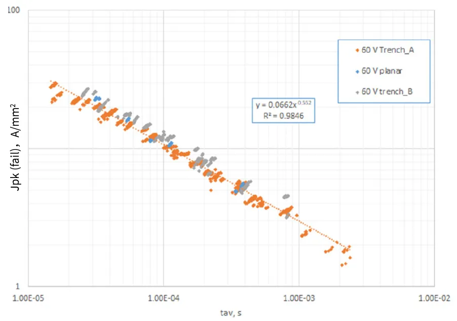
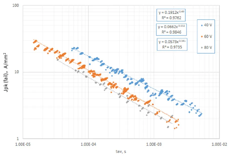
In Figure 1 the y-axis is labeled Jpk(fail) in A/mm2, which is Ipk(fail) divided by the device active area. This allows Ipk(fail) versus tav data from devices with active die areas ranging from about 1 mm2 to 13 mm2 to be compared. The plot includes three distinct 60 V MOSFET technologies with similar avalanche voltage characteristics. The data show that technologies with similar avalanche voltage behavior exhibit the same UIS capability when normalized to active die area (or, more precisely, active die volume). Figure 2 shows Jpk(fail) versus tav for three different BV ratings. Lower-BV devices (lower Vav) show higher Jpk capability at a given avalanche time compared with higher-BV devices. However, if the same data are plotted as failure energy density (J/mm2), the energy density function is roughly the same regardless of technology or BV rating, further supporting that MOSFET UIS capability scales with active die volume.
Non-Thermal Failures and Internal npn Activation
MOSFET UIS capability is generally limited by device thermal capacity, but there is an exception. At high avalanche current density, devices can fail at levels far below the thermal-limited Jpk(fail). The cause is the internal npn transistor formed by the p-doped body region, n-doped source region, and n-doped drift (epi) region. The body-to-source junction forms the base-emitter path and is shorted to the source metal at the front side. Therefore, the source metal contact design and process are critical parameters for UIS capability. If the internal npn is forward biased because the body-to-source junction becomes forward biased, avalanche current can concentrate at a defect and rapidly activate the npn, causing destruction. The finite resistance of the p-doped body region means that at sufficiently high avalanche current densities the p-n junction will become forward biased and activate the npn transistor.
Every power MOSFET has a maximum limiting peak avalanche current, even if the datasheet does not explicitly list a maximum UIS Ipk. In applications where the device must interrupt very high short-circuit currents, the maximum Ipk during avalanche can be a limiting factor. Because of small stray inductances in PCB traces or power wiring, a MOSFET may avalanche destructively during turn-off even when the avalanche energy is well below the device thermal failure energy.
Repeated Avalanche Operation and HCI Effects
Power MOSFETs can be operated repeatedly into avalanche provided each event remains within safe operating limits (Ipk, tav, Tj(initial)). However, groove-based MOSFET technologies can exhibit DC parameter shifts when subjected to repeated avalanche because of hot-carrier injection-like effects. During avalanche, the drift (n-epi) region under high field can conduct high current density. In groove structures, the gate and shielding oxides are adjacent to the region of high avalanche current; the high fields can inject charge carriers into the gate and shielding oxides depending on operating conditions. Planar technologies do not share this adjacency and are typically not affected by repeated avalanche HCI in the same way. Consequently, planar MOSFETs are generally less susceptible to repeated-avalanche-induced parameter shifts.
Parameters affected by repeated avalanche HCI include BVdss (avalanche voltage), Idss (off-state drain-source leakage), Vth (threshold voltage), and Rds(on). Igss (off-state gate-source leakage) is not affected by repeated avalanche. BVdss shifts usually occur and stabilize after the first several hundred to several thousand avalanche cycles; the magnitude of shift is typically less than ±3 V in most cases. After millions to hundreds of millions of cycles, Idss can increase significantly, from the nA range to single-digit μA. Channel mobility can be degraded by repeated-avalanche HCI, leading to increased Rds(on) and reduced Vth after many millions to hundreds of millions of cycles. Whether these shifts are significant depends on the specific repeated-avalanche conditions: average and peak junction temperature, temperature swing, avalanche current density, avalanche duration, and the number of cycles. Typically, these shifts do not cause immediate device failure, but the direction and magnitude of parameter changes can create application-level problems.
There is no standardized method to specify a MOSFET's repetitive avalanche capability. Any repetitive-avalanche rating on a datasheet should be based on assumed operating conditions and should define the method used to determine capability limits, for example the number of cycles required to produce a given percentage change in specific DC parameters.
Design Recommendations
As a general design rule, repetitive avalanche operation should be avoided where possible. However, in many real-world applications MOSFETs are expected to undergo repetitive avalanche as part of normal operation. In those cases, the device suitability should be evaluated empirically under representative application conditions.
UIS/UIL is a specific form of MOSFET avalanche caused by turn-off into an unclamped inductive load. MOSFET design and manufacturing make UIS avalanche behavior limited by either device thermal capacity or the maximum peak avalanche current density. The best representation of MOSFET UIS capability is the Ipk versus tav SOA curve. Single UIS energy ratings should not be used to compare devices unless the test conditions (Ipk, Vav, L, tav, and Tj(initial)) are known and understood. Devices with similar avalanche voltage function and similar thermal capacity will exhibit similar UIS failure behavior, though derating factors on Ipk versus tav SOA curves may vary by industry practice. Safe repetitive avalanche operation is possible, but DC parameter shifts may occur depending on operating conditions.