ALLPCB


Introduction
As semiconductor fabrication has advanced, Moore's law became a guiding observation: the number of transistors on an integrated circuit roughly doubles every 18 to 24 months. Over roughly 70 years since the 1950s, process technologies have evolved to include BJT, MOSFET, CMOS, DMOS and hybrid processes such as BiCMOS and BCD, driven by the goal of producing smaller, more reliable transistors.
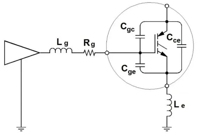
1. BJT
The bipolar junction transistor (BJT), commonly called a transistor, is a bipolar device in which current flow involves both electrons and holes. Charge transport is governed by diffusion and drift across PN junctions.
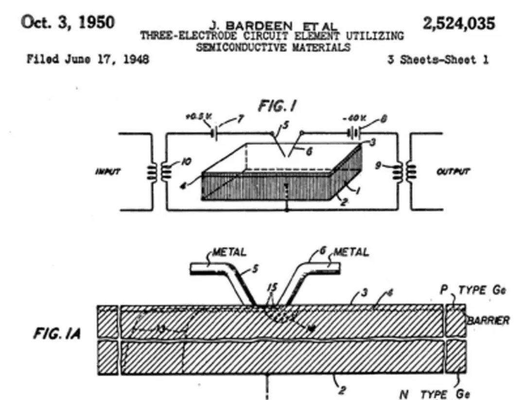
The first point-contact transistor was demonstrated in December 1947 by John Bardeen and Walter Brattain at Bell Labs. Shortly afterward, William Shockley proposed and patented the junction transistor in 1948 and published its working theory in 1949. Bell Labs developed manufacturing processes that enabled junction transistors to be mass produced around 1951. Shockley, Bardeen and Brattain were awarded the 1956 Nobel Prize in Physics for their contributions.
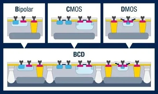
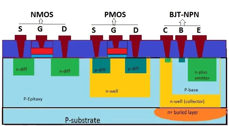
Common BJT types are NPN and PNP. Structurally, the emitter region is heavily doped, the base region is very thin and lightly doped, and the collector region has a large area with light doping.
Advantages of BJT technology include high response speed, high transconductance (large output current change for input voltage change), low noise, high analog accuracy and strong current driving capability. Disadvantages include lower integration density (vertical depth limits scaling), and higher power consumption.
Related Reading: BJT Structure and Operating Principles
2. MOS
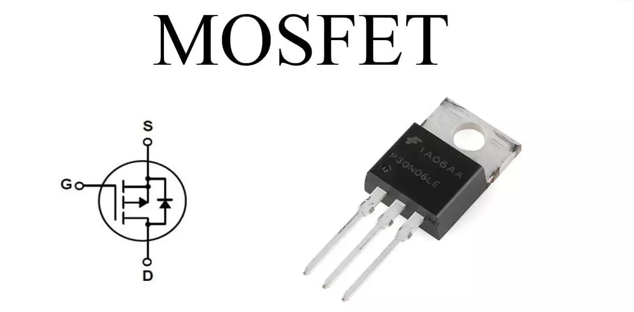
The metal-oxide-semiconductor field-effect transistor (MOSFET) controls a conductive channel in the semiconductor by an electric field applied to a gate electrode separated by an insulating oxide (typically SiO2). Because the gate is insulated from source and drain, MOSFETs are also called insulated-gate FETs. Bell Labs announced a working MOS structure in 1962, a milestone that underpinned later semiconductor memories.
MOSFETs are classified by channel type (N-channel or P-channel) and by gate-bias behavior: depletion-type devices have a channel at zero gate voltage, while enhancement-type devices require a gate voltage of appropriate polarity to create a channel. Power MOSFETs are typically N-channel enhancement devices.
BJTs are bipolar devices where both minority and majority carriers participate in conduction; they are current-controlled and tend to have higher power consumption. MOSFETs are unipolar devices that conduct via majority carriers and are voltage-controlled, typically exhibiting lower power consumption and lower on-resistance (often a few hundred milliohms). For many switching applications, MOSFETs are used because of higher efficiency. In cost-sensitive, low-power-insensitive scenarios, BJTs may still be chosen for price reasons.
Related Reading: Understanding MOSFET Parameters
3. CMOS
Complementary metal-oxide-semiconductor (CMOS) technology uses complementary P-channel and N-channel MOSFETs to construct circuits and logic gates. A common example is the CMOS inverter used to convert logic 1->0 or 0->1.
The typical CMOS cross-section shows an NMOS and a PMOS with their gates tied together as the input and their drains tied together as the output. VDD connects to the PMOS source and VSS to the NMOS source.
Wanlass and Sah at Fairchild Semiconductor demonstrated CMOS circuits in the early 1960s, and RCA developed one of the first CMOS integrated circuits in 1968. CMOS advantages include low static power consumption and high integration density (with STI/LOCOS process options to further improve density). A notable disadvantage is susceptibility to latch-up, where parasitic structures can form conducting paths between rails under disturbance.
4. DMOS
Double-diffused MOS (DMOS) uses a dual-diffusion process and a structure similar to MOSFETs but with higher drain breakdown voltage. A standard N-channel DMOS cross-section is commonly used for low-side switch applications where the source is tied to ground. P-channel DMOS devices are used for high-side applications with the source tied to a positive rail. Complementary DMOS devices combine N- and P-channel DMOS on the same chip to provide complementary switching functions.
DMOS can be classified by channel orientation: vertical double-diffused MOSFET (VDMOS) has a vertical channel and typically offers higher breakdown voltage and current handling versus lateral DMOS (LDMOS), though on-resistance can still be relatively high.
Compared with conventional MOSFETs, DMOS devices provide higher conduction capability and lower resistance, making them widely used in high-power electronics such as power switches, power tools, and electric vehicle drivers.
5. BiCMOS
BiCMOS integrates bipolar transistors and CMOS on the same chip. The approach uses CMOS as the primary logic and digital circuitry while adding bipolar devices where high-speed or strong current drive is required for large capacitive loads. BiCMOS combines CMOS low-power, high-density advantages with BJT high-speed and drive capability.
6. BCD
BCD (Bipolar-CMOS-DMOS) integrates bipolar, CMOS and DMOS devices on a single chip, enabling analog, logic and power functions in one process. BCD processes have been developed for applications such as power management, analog data acquisition and power actuators. Mature BCD process nodes are commonly around 100 nm, with smaller nodes such as 90 nm in prototype and 40 nm under development.