ALLPCB


Overview
In bipolar junction transistors both polarities of charge carriers participate in conduction, so they are called bipolar transistors. Another transistor class uses a single carrier type for conduction and is therefore called unipolar; since it is controlled mainly by an electric field, it is called a field-effect transistor (FET). FETs are broadly divided into junction FETs (JFET) and insulated-gate FETs (MOSFET).
On general marketplaces and in common catalogs, the term "FET" most often refers to insulated-gate MOSFETs. JFETs are less common in modern applications, so this article focuses on MOSFET basics and practical use.
MOSFET Types and Characteristics
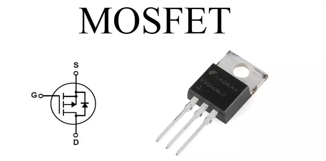
The full name is metal-oxide-semiconductor field-effect transistor. Because the gate is isolated by an insulating layer, it is called an insulated-gate FET; its common abbreviation is MOSFET. MOSFETs have very high input impedance. By channel type they are N-channel or P-channel, and each can be either enhancement-mode or depletion-mode. N-channel MOSFETs are commonly referred to as NMOS, and P-channel MOSFETs as PMOS.
Pins, Substrate and Parasitic Diode
MOSFETs have three main terminals: gate (G), drain (D) and source (S). The substrate (body) is typically tied to the source internally. There is usually a parasitic diode between drain and source; in circuit symbols the diode orientation aligns with the device arrow direction. In practical designs the enhancement-mode N-channel and P-channel MOSFETs are used most often; depletion-mode parts are less common.
Using a MOSFET as an Electronic Switch
MOSFETs are voltage-controlled devices: they require a gate-to-source voltage V_GS to turn on rather than a continuous gate current. For an N-channel enhancement MOSFET the device conducts when V_GS exceeds the threshold voltage V_GS(th), typically around 2 to 4 V for many devices. For a P-channel enhancement MOSFET the device conducts when V_GS is below a negative threshold, typically around -2 to -4 V.
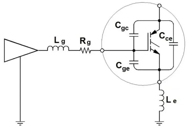
Gate Resistor and Parasitic Capacitances
The gate is separated from the channel by an insulating silicon dioxide layer, which forms a capacitance between gate and source (Cgs) and between gate and drain (Cgd). These parasitic capacitances are unavoidable and depend on device construction, materials and applied voltages. If there is no resistor from gate to source (Rgs), applying a gate voltage charges Cgs and the gate can retain that voltage even after the control signal is removed, leaving the MOSFET conducting.
Adding a gate-to-source resistor Rgs provides a discharge path for Cgs when the drive is removed, allowing the MOSFET to turn off reliably. Including Rgs helps prevent unintended turn-on when the gate drive is absent, improving circuit reliability.
Applications and Key Properties
MOSFETs feature high input impedance, fast switching speed, good thermal stability and voltage-controlled current. In circuits they are commonly used as switches and as amplifier devices. There is much more to MOSFET design and application (drive circuits, Rds(on), switching losses, safe operating area, etc.), which can be discussed separately.