ALLPCB


Basic composition and bonding
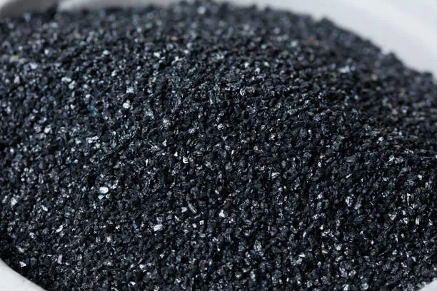
Silicon carbide (SiC) is a binary compound of silicon (Si) and carbon (C) in a 1:1 ratio, with a basic structural unit of Si–C tetrahedra. Silicon atoms are relatively large compared with carbon atoms; a simple analogy is to compare Si atoms to apples and C atoms to oranges, stacking equal numbers of each to form the SiC crystal.
The Si–Si nearest-neighbor distance in related silicon structures is about 3.89 ?. Modern photolithography can reach roughly 3 nm resolution (about 30 ?), so lithography resolution is on the order of several times typical atomic spacings.
The Si–Si bond energy is about 310 kJ/mol; the Si–C bond distance is about 1.89 ? and the Si–C bond energy is about 447 kJ/mol. The larger Si–C bond energy indicates that SiC is chemically more stable than conventional silicon-based semiconductor materials. In the SiC crystal, each C atom is bonded to four nearest Si atoms, and each Si atom is bonded to four nearest C atoms.
Layered description and polytypes
The SiC crystal can also be described using a layered model: certain C atoms occupy hexagonal close-packed sites within a given plane to form a close-packed C layer, while Si atoms occupy analogous close-packed sites in a separate plane to form a Si layer. Each atom in a C close-packed layer is bonded to the nearest Si atoms in adjacent layers, and vice versa.
Two adjacent C and Si close-packed layers form one Si–C biatomic layer. SiC exhibits a large number of polytypes; over 200 polytypes have been identified. Although the basic tetrahedral building blocks are the same, different stacking sequences produce different crystal forms. The Ramsdell notation is commonly used to designate SiC polytypes; it combines a number indicating the repeat period of Si–C bilayers with a letter indicating the lattice type.
In Ramsdell notation, "C" denotes the cubic polytype, "H" denotes hexagonal, and "R" denotes rhombohedral. Except for 2H-SiC and 3C-SiC, most polytypes can be regarded as mixtures of zincblende and wurtzite stacking, i.e. variations of close-packed hexagonal arrangements.
C-face vs Si-face and their consequences
The C-face refers to the (000-1) plane of a SiC wafer, the surface obtained by cutting the crystal along the negative direction of the c axis, where the terminating atoms are carbon. The Si-face refers to the (0001) plane, the surface cut along the positive c-axis direction, where the terminating atoms are silicon.
The choice of C-face or Si-face influences SiC physical and electrical properties such as thermal conductivity, electrical conductivity, carrier mobility, and interface state density. It also affects device fabrication steps and performance, including epitaxial growth, ion implantation, oxidation, metal deposition, and contact resistance.