ALLPCB


Role of registers and buffers near converters
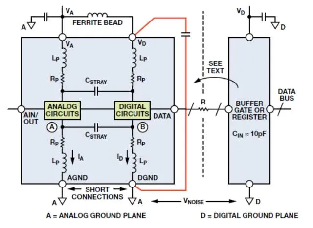
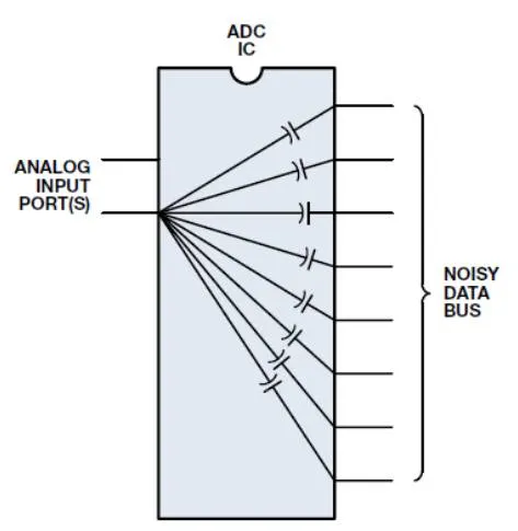
Although many converters have tri-state outputs/inputs, registers frequently remain on the chip. They allow data pins to couple signals into sensitive regions, so isolating buffers remain a good design practice. In some cases, additional data buffers located on the analog ground plane adjacent to the converter outputs are required to provide better isolation.
Placing data buffers next to the converter helps isolate digital outputs from data-bus noise (see Figure 1). Buffers also reduce the load seen by the converter digital outputs while providing a Faraday-like shield between the digital outputs and the data bus (see Figure 2).
Series resistor and RC filtering
The series resistor between the ADC output and the buffer register input (labeled "R" in Figure 1) helps minimize digital transient currents that can affect converter performance. The resistor isolates the digital output driver from the input capacitance of the buffer register. In addition, the RC network formed by the series resistor and the buffer input capacitance acts as a low-pass filter to slow fast edges.
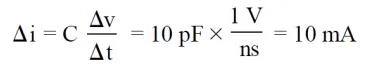
A typical CMOS gate combined with PCB traces and vias produces roughly 10 pF of load. Without an isolation resistor, a logic output with a 1 V/ns slew rate will produce a 10 mA dynamic current. Using a series resistor of about 500 ohms to drive a 10 pF register input reduces the transient output current and results in approximately 11 ns rise and fall times.
TTL registers have higher input capacitance and can significantly increase dynamic switching currents, so their use should be avoided where possible.
Grounding and decoupling for buffers and digital circuits
Buffer registers and other digital circuits should be grounded and decoupled to the PCB digital ground plane. Any noise between analog and digital ground planes reduces noise margin on the converter's digital interface. Digital noise immunity is often on the order of hundreds to thousands of millivolts, so small noise levels are usually acceptable. If noise on the digital ground plane relative to the analog ground plane exceeds a few hundred millivolts, reduce the digital ground impedance to maintain acceptable digital noise margins. Under no circumstances should the voltage between the two ground planes exceed 300 mV, as the IC may be damaged.
Separate power supplies for analog and digital circuits are recommended. The analog supply should be used to power the converter. If the converter specifies a separate digital power pin (VD), it should be powered from an isolated analog supply or be filtered as shown in Figure 3. All converter power pins should be decoupled to the analog ground plane; all logic circuit power pins should be decoupled to the digital ground plane. If the digital supply is relatively quiet, it may be used to power analog circuits, but extreme care is required.
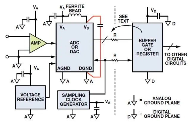
In some cases VD cannot be tied to the analog supply. Some high-speed ICs power their analog circuitry from +5 V while using +3.3 V or lower for their digital interface to match external logic. In that case, the IC's +3.3 V pin should be decoupled directly to the analog ground plane. It is also recommended to place a ferrite bead in series with the power trace to the +3.3 V digital logic supply. The sampling-clock circuitry should be treated like the analog circuits: grounded and extensively decoupled to the analog ground plane.
Ground return paths at high frequency
Power and signal currents are best returned via a ground plane, which also provides reference nodes for converters, reference sources, and other subcircuits. However, using a ground plane does not guarantee a high-quality AC ground reference in all cases.
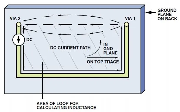
Consider the simple two-layer PCB example in Figure 4: a DC/AC current source on the top layer connects to via 1 at one end and via 2 through a U-shaped copper trace at the other. Both vias pass through the board to the ground plane. Ideally, the ground loop impedance between the top connector and vias 1 and 2 would be zero and the voltage across the current source zero.
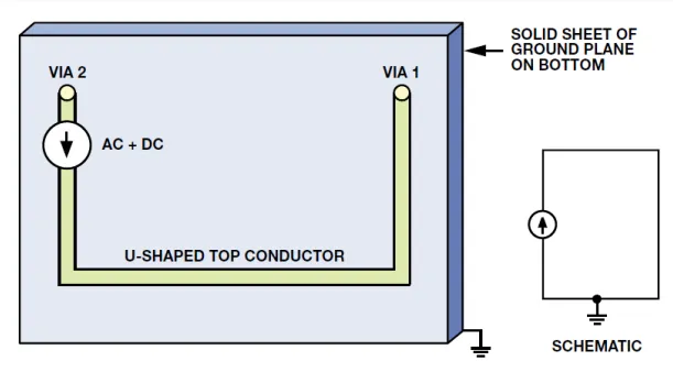
Understanding how current travels in the ground plane from via 1 to via 2 helps reveal real-world issues and ways to eliminate high-frequency ground noise in layouts.
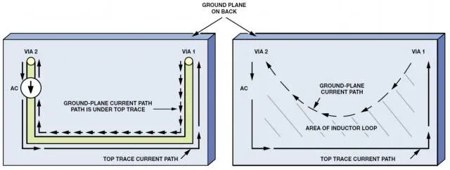
For DC currents the return follows the path of least resistance through the ground plane, as shown in Figure 5. Some current spreading occurs, but the bulk of the current follows the lowest-resistance path. By contrast, AC currents follow the path of least impedance, which depends on inductance.
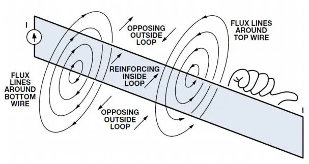
Inductance is proportional to the loop area; the relationship is illustrated with the right-hand rule and magnetic field lines in Figure 6. Inside the loop, magnetic fields from all portions of the loop reinforce each other; outside the loop they tend to cancel. The magnetic field is therefore largely confined to the loop. A larger loop area means greater inductance, which stores more magnetic energy (Li^2) for a given current and presents higher impedance (XL = jωL), producing larger voltages at a given frequency.
The current will take the path of lowest impedance in the ground plane. Considering the loop formed by the U-shaped surface trace and the ground plane underneath, and neglecting resistance, high-frequency AC returns flow along the path that minimizes loop area.
In the example, the smallest loop area is clearly formed by the U-shaped top trace and the section of ground plane directly beneath it. Figure 5 shows the DC return path, while Figure 7 shows the AC return, which is the small-area path directly under the U-shaped top trace. In practice, ground plane resistance causes low-to-mid-frequency currents to divide between the direct return path and the area directly under the top trace. Even at frequencies as low as 1 MHz or 2 MHz, the return path is close to the top trace.
Sampling-clock considerations
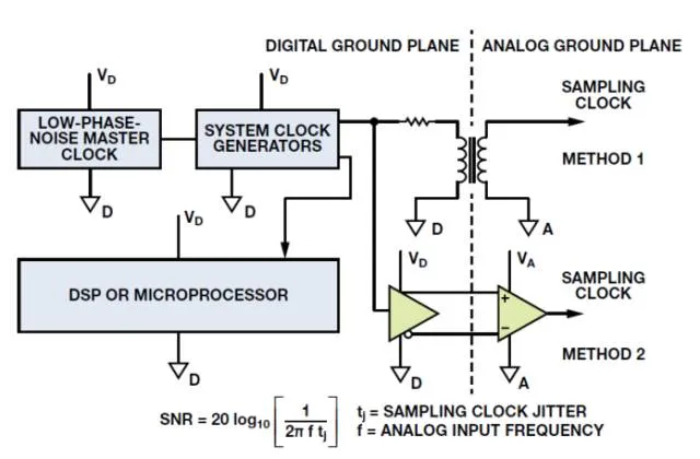
For high-performance sampling systems, use a low-phase-noise crystal oscillator to generate the ADC or DAC sampling clock, because sampling-clock jitter modulates the analog input/output and raises the noise and distortion floor. The sampling-clock generator should be isolated from noisy digital circuits and grounded and decoupled to the analog ground plane, alongside the analog amplifiers and ADC.
The effect of sampling-clock jitter on ADC signal-to-noise ratio (SNR) can be approximated by the formula shown in the original figure:
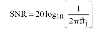
In the formula, f is the analog input frequency and SNR is the SNR of an otherwise ideal infinite-resolution ADC when the only noise source is rms sampling-clock jitter tj. For example, with tj = 50 ps rms and f = 100 kHz, SNR = 90 dB, corresponding to roughly 15 bits of dynamic range.
Note that tj in the example is the root-sum-square of external clock jitter and the ADC's internal aperture jitter. In most high-performance ADCs, internal aperture jitter is negligible compared to external clock jitter.
Because SNR degradation is primarily caused by external clock jitter, the sampling clock must be as noise-free as possible with the lowest achievable phase jitter. This requires using a crystal oscillator. Compact crystal oscillators that provide low jitter (under about 5 ps rms) with CMOS-compatible outputs are available from multiple suppliers.
Ideally, the sampling-clock crystal oscillator should reference the analog ground plane in a split-ground system. System constraints may require deriving the sampling clock from a higher-frequency, multi-use system clock on the digital ground plane and then routing it from the digital ground reference to the ADC on the analog ground plane. Noise between the two ground planes is added directly to the clock and increases jitter, which reduces SNR and can create spurious harmonics.
Transmitting the sampling clock as a differential signal can mitigate this problem. Use a small RF transformer (as shown in Figure 8) or high-speed differential drivers and receivers. If using differential logic drivers/receivers, choose technologies (for example, ECL/PECL) that minimize phase jitter. In single +5 V systems, ECL-style outputs can be tied between ground and +5 V (PECL) and AC-coupled to the ADC sampling input. Regardless of the transport method, the system master clock should originate from a low-phase-noise crystal oscillator.