ALLPCB


Introduction
As chip designs become more complex and power constraints tighten, single-clock designs are increasingly rare. Most chips are driven by multiple, and sometimes dozens or hundreds of, asynchronous clocks. Whenever multiple clocks are present, designers must address clock domain crossing (CDC) issues; a primary concern in such designs is metastability.
1. Metastability
1.1 What is metastability
Metastability refers to a condition during normal circuit operation in which a signal does not resolve to a stable 0 or 1 within a bounded time. In multi-clock designs metastability is unavoidable. The goal is to reduce its occurrence and propagation and to mitigate its harmful effects.
1.2 Why metastability occurs
Storage elements such as cross-coupled inverters, SR latches, D latches, and D flip-flops have two stable states, 0 and 1, which allow them to store a bit. Metastability is a state that is neither a firm 0 nor 1, or where the eventual state cannot be determined with certainty. This arises because real devices are not ideal: they can exhibit analog behavior during transitions. For example, an ideal CMOS inverter has a well-defined voltage transfer characteristic, but actual devices can take nonideal paths through that characteristic when inputs change near timing thresholds.
1.3 Hazards of metastability
Before resolving to a stable logic level, a metastable output may glitch, oscillate, or sit at an intermediate analog voltage. Besides causing logic misinterpretation, an intermediate voltage can induce metastability in downstream stages, causing propagation of the condition. Design techniques such as Gray-code counters in asynchronous FIFOs can reduce the impact of logic misinterpretation, but propagation of metastability enlarges the fault surface and is harder to control.
1.4 Quantifying metastability
Because metastability cannot be completely eliminated, designers quantify its risk using mean time between failures (MTBF). MTBF estimates the average time between events where metastability leads to a system-level failure; a higher MTBF indicates a more robust design. The MTBF for a register can be calculated using standard metastability models and parameters such as resolution time constant, setup/hold violation window, clock frequency, and asynchronous input toggle rate.
1.5 Reducing metastability
Metastability is an intrinsic property of physical devices and cannot be entirely removed. However, adherence to established design rules can reduce its occurrence and propagation, and mitigate its effects. With proper synchronization and timing practices, even large-scale processors and accelerators can be designed to make metastability-induced failures extremely unlikely.
2. Synchronizers
2.1 Sampling across clock domains
A common misconception is that a signal crossing clock domains must be sampled by every receiving clock edge without missing any value. In practice, designers must explicitly consider sampling requirements and choose synchronization strategies that preserve the necessary semantics for the signal being transferred.
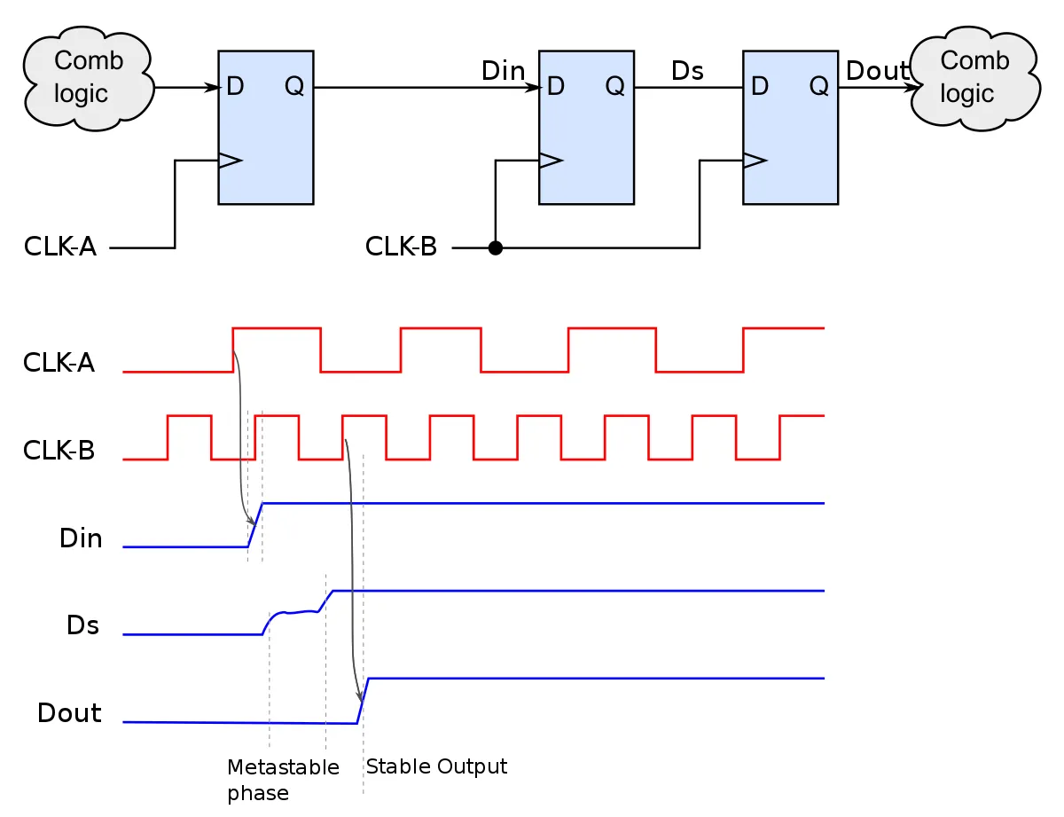
2.2 Two-stage flip-flop synchronizer
The simplest and most widely used synchronizer is the two-stage flip-flop chain: an asynchronous source feeds a first flip-flop in the destination clock domain, whose output then feeds a second flip-flop. This gives the first flop additional time to resolve any metastability before its value is used elsewhere in the destination domain.
2.3 Three-stage or multi-stage synchronizers
At very high speeds or for particularly critical signals, a two-stage synchronizer may not provide sufficient MTBF. In such cases a three-stage or multi-stage synchronizer is used to increase the effective resolution time and improve MTBF. MTBF for two- and three-stage flip-flop synchronizers can be calculated using established formulas that account for stage count, resolution time constant, clock period, and input toggling characteristics.
2.4 Synchronizer input: register at the source clock
Another common requirement when using synchronizers is that the signal crossing clock domains should originate from a register clocked by the source domain. In other words, the cross-domain signal should be the output of a register; it should not pass through combinational logic between the source register and the synchronizer input. This practice reduces the effective uncertainty window and improves synchronization reliability.
3. Conclusion
Clock-domain crossing is one of the most important topics in chip design. Understanding metastability and how to use synchronizers is a foundational part of CDC design. A solid grasp of these concepts is necessary to apply CDC techniques effectively and to design robust multi-clock systems.