In the fast-paced world of PCB assembly, precision is everything. If you're looking to optimize solder paste application for mixed-component boards, step-up stencils are a game-changer. These specialized tools allow for varying thicknesses in a single stencil, ensuring the right solder paste volume for both large and small components. This guide dives deep into step-up stencil design rules, solder paste volume control, manufacturing processes, inspection techniques, and troubleshooting tips to help you achieve flawless PCB assembly results.
Whether you're an engineer refining your surface mount technology (SMT) process or a manufacturer aiming to reduce defects, this comprehensive resource will walk you through every aspect of step-up stencils. Let’s explore how to master this critical tool for high-quality PCB production.
What Are Step-Up Stencils and Why Do They Matter?
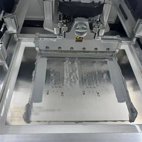
Step-up stencils are a type of solder paste stencil used in SMT assembly with varying thicknesses across different areas. Unlike traditional stencils with uniform thickness, step-up stencils feature thicker regions (step-up areas) to deposit more solder paste for larger components like connectors or power devices, while thinner regions cater to fine-pitch components requiring less paste. This design addresses the challenge of mixed-component PCBs where a one-size-fits-all stencil fails to deliver optimal results.
The importance of step-up stencils lies in their ability to prevent common soldering defects such as insufficient solder joints on large components or bridging on smaller ones. By tailoring solder paste volume to specific component needs, they enhance assembly reliability and reduce rework costs. For modern electronics with high-density layouts and diverse component sizes, mastering step-up stencils can significantly boost production efficiency.
Step-Up Stencil Design Rules: Building the Foundation
Designing a step-up stencil requires careful planning to ensure it meets the needs of your PCB layout. Here are the key design rules to follow for optimal performance:
- Determine Thickness Variations: Identify which components need more solder paste (e.g., large connectors may require a thickness of 0.15 mm) and which need less (e.g., fine-pitch ICs may need 0.1 mm). A typical step-up difference is 0.025 to 0.05 mm, but this varies based on component specifications.
- Aperture Sizing: Aperture dimensions should match the pad size with slight reductions (often 10-20% smaller) to prevent excess paste. For step-up areas, slightly larger apertures can accommodate the increased volume.
- Transition Zones: Ensure smooth transitions between step-up and standard thickness areas to avoid paste leakage or uneven deposition. A gradual slope or chamfered edge in the stencil can help.
- Component Proximity: Avoid placing step-up regions too close to fine-pitch components (maintain at least 2-3 mm separation) to prevent interference during printing.
- Stencil Material: Use high-quality stainless steel with laser-cut precision to ensure durability and accuracy, especially in step-up regions where stress concentration is higher.
Following these rules during the design phase sets the stage for effective solder paste application. Always collaborate with your design team to align stencil specifications with the PCB layout and component requirements.
Step-Up Stencil Solder Paste Volume: Getting the Balance Right
Controlling solder paste volume is the primary goal of a step-up stencil. Too little paste on large components can lead to weak joints, while too much on small components risks bridging or shorts. Here's how to achieve the right balance:
- Calculate Volume Needs: Use the formula for solder paste volume: Volume = Aperture Area x Stencil Thickness. For a step-up area with a thickness of 0.15 mm and an aperture of 2 mm x 2 mm, the volume is 0.6 mm3. Compare this to component datasheets to ensure it meets joint requirements.
- Adjust for Component Type: Larger components like I/O connectors often need 30-50% more paste volume than standard SMT parts. Fine-pitch components (e.g., 0.4 mm pitch QFNs) may require 20-30% less to avoid excess.
- Test and Validate: Conduct trial runs with different step-up heights to measure paste transfer efficiency. Aim for a transfer efficiency of 80-90%, adjusting thickness or aperture if needed.
- Consider Paste Type: The viscosity and particle size of solder paste (e.g., Type 3 or Type 4) impact deposition. Thicker pastes may require slight increases in step-up height to ensure proper flow.
By fine-tuning solder paste volume through step-up stencil design, you can achieve consistent soldering results across diverse components, minimizing defects and improving yield.
Step-Up Stencil Manufacturing Process: From Concept to Reality
The manufacturing of step-up stencils is a precise process that directly affects their performance in PCB assembly. Understanding the steps involved can help you select a reliable stencil provider and ensure quality. Here’s how step-up stencils are made:
- Design File Preparation: Start with a detailed Gerber file or stencil layout specifying step-up areas, thicknesses, and aperture locations. Ensure the file includes fiducial marks for alignment during printing.
- Material Selection: High-grade stainless steel (typically 0.1-0.2 mm thick) is chosen for its durability and resistance to wear. Nickel plating may be added for enhanced longevity.
- Laser Cutting: Apertures are cut using high-precision laser technology to achieve accuracies within ±0.005 mm. This ensures exact paste deposition, especially in step-up regions.
- Step Formation: Step-up areas are created by chemically etching or mechanically milling the stencil to increase thickness in designated zones. Advanced processes ensure smooth transitions between thicknesses.
- Polishing and Finishing: The stencil surface is polished to reduce friction during printing, ensuring clean paste release. Edges are deburred to prevent damage to squeegees or PCBs.
- Quality Control: Final stencils undergo dimensional checks using optical inspection tools to verify thickness variations and aperture accuracy before shipment.
Partnering with a trusted manufacturer who follows these steps ensures your step-up stencil meets the tight tolerances required for modern PCB assembly.
Step-Up Stencil Inspection: Ensuring Precision and Reliability
Inspection is a critical step to confirm that a step-up stencil performs as intended. Poorly inspected stencils can lead to printing errors and costly rework. Follow these inspection practices to maintain quality:
- Visual Inspection: Check for surface defects, scratches, or burrs that could affect paste transfer. Ensure step-up transitions are smooth and free of sharp edges.
- Dimensional Verification: Use a precision micrometer or 2D/3D measurement system to verify stencil thickness in step-up and standard areas. Tolerances should be within ±0.01 mm of the design spec.
- Aperture Accuracy: Inspect aperture sizes and shapes under a microscope or with automated optical inspection (AOI) tools to ensure they match the design file within ±0.005 mm.
- Alignment Check: Verify fiducial marks and overall stencil dimensions align with the PCB layout to prevent misalignment during printing.
- Test Printing: Perform a test run on a sample PCB to evaluate paste deposition in step-up areas. Look for uniform paste height and volume, adjusting the stencil if discrepancies are found.
Regular inspection not only validates stencil quality but also extends its lifespan by identifying wear or damage early. Incorporate these checks into your standard operating procedures for consistent results.
Step-Up Stencil Troubleshooting: Solving Common Issues
Even with the best design and manufacturing, issues can arise during step-up stencil use. Here are common problems and how to address them effectively:
- Insufficient Solder Paste in Step-Up Areas: If large components lack enough paste, check if the step-up thickness or aperture size is adequate. Increase thickness by 0.025 mm or widen apertures by 5-10% if needed. Also, ensure the squeegee pressure is sufficient (typically 3-5 kg) for paste transfer.
- Excess Paste on Fine-Pitch Components: Over-deposition near step-up zones can cause bridging. Reduce stencil thickness outside step-up areas or adjust paste viscosity. Adding a barrier or keep-out zone around fine-pitch parts can help.
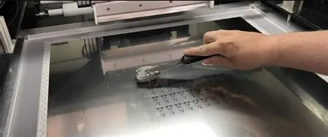
- Uneven Paste Deposition: This often results from poor stencil-to-PCB contact. Verify printer alignment and ensure the stencil is clean and free of residue. Adjust snap-off distance (typically 0.5-1 mm) for better contact.
- Stencil Wear in Step-Up Regions: Repeated use can degrade step-up areas faster. Inspect for thinning or deformation after 10,000-15,000 prints and replace the stencil if tolerances exceed ±0.01 mm.
- Paste Leakage at Transitions: If paste leaks between step-up and standard areas, the transition slope may be too steep. Work with your stencil provider to refine the etching process for smoother gradients.
By systematically addressing these issues, you can maintain high-quality solder paste printing and minimize production downtime. Documenting troubleshooting outcomes can also help refine future stencil designs.
Benefits of Mastering Step-Up Stencils in PCB Assembly
Investing time and effort into mastering step-up stencils offers several advantages for PCB assembly:
- Improved Soldering Quality: Precise solder paste volume reduces defects like open joints or shorts, ensuring reliable electrical connections.
- Cost Efficiency: Fewer defects mean less rework and scrap, saving time and materials in high-volume production.
- Versatility: Step-up stencils accommodate complex PCB designs with mixed components, making them ideal for IoT devices, automotive electronics, and consumer products.
- Enhanced Durability: Properly designed and maintained stencils last longer, providing consistent performance over thousands of prints.
These benefits translate to higher customer satisfaction and a stronger competitive edge in the electronics manufacturing industry.
Best Practices for Using Step-Up Stencils
To maximize the effectiveness of step-up stencils, adopt these best practices in your workflow:
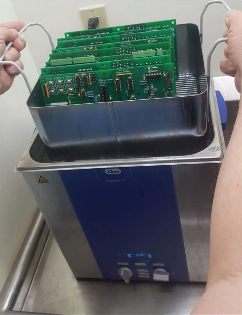
- Regularly clean the stencil after every 5-10 prints using isopropyl alcohol and a lint-free cloth to prevent paste buildup.
- Store stencils flat in a protective case to avoid bending or damage to step-up areas.
- Calibrate your printer settings (squeegee speed of 20-50 mm/s, pressure of 3-5 kg) to match the stencil’s unique profile.
- Work closely with your stencil manufacturer to iterate designs based on production feedback and evolving PCB requirements.
Implementing these habits ensures consistent performance and extends the usability of your step-up stencils.
Conclusion: Elevate Your PCB Assembly with Step-Up Stencils
Step-up stencils are an indispensable tool for modern PCB assembly, offering precise control over solder paste volume for diverse component types. By adhering to step-up stencil design rules, optimizing solder paste volume, understanding the manufacturing process, conducting thorough inspections, and applying effective troubleshooting techniques, you can achieve superior soldering results and streamline your production process.
At ALLPCB, we’re committed to supporting engineers and manufacturers with cutting-edge solutions for SMT assembly. Whether you’re tackling high-density designs or mixed-component challenges, mastering step-up stencils can elevate your PCB quality to new heights. Start implementing these strategies today and witness the difference in your assembly outcomes.
 ALLPCB


