 ALLPCB


In the fast-evolving world of electronics, ensuring the reliability and functionality of integrated circuits (ICs) is more critical than ever. Design for Test (DFT) is a cornerstone of this process, enabling engineers to detect manufacturing defects and operational faults early in the development cycle. If you're looking to master advanced DFT techniques, modern DFT tools, automation, test pattern generation (ATPG), and DFT best practices in 2025, you're in the right place. This comprehensive guide will walk you through the latest strategies and solutions to optimize your testing processes and enhance product reliability.
What Is Design for Test (DFT) and Why Does It Matter in 2025?
Design for Test, or DFT, refers to a set of design methodologies that make ICs easier to test for defects during manufacturing and operation. By embedding testability features into the design, DFT reduces testing time, cuts costs, and improves fault coverage. In 2025, as chip complexity continues to soar with smaller geometries (like 3nm and below) and multi-billion transistor designs, DFT has become indispensable for maintaining quality and yield.
The rise of Internet of Things (IoT) devices, artificial intelligence (AI) hardware, and 5G technologies demands chips with near-zero defect rates. Without robust DFT strategies, identifying faults in such intricate systems becomes a costly and time-consuming challenge. This blog dives deep into advanced DFT techniques and modern tools to help engineers stay ahead in this competitive landscape.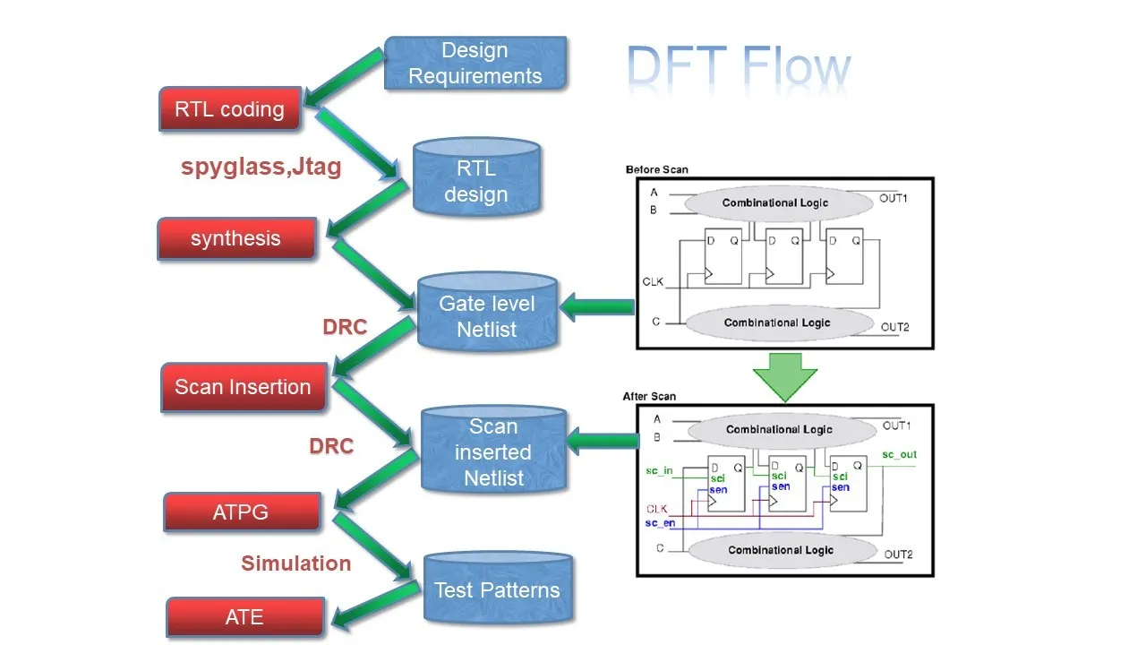
The Importance of Advanced DFT Techniques in Modern Chip Design
As IC designs grow more complex, traditional testing methods fall short. Advanced DFT techniques address these challenges by improving test coverage and reducing test time. Here are some cutting-edge approaches shaping the industry in 2025:
1. Hierarchical DFT for Large Designs
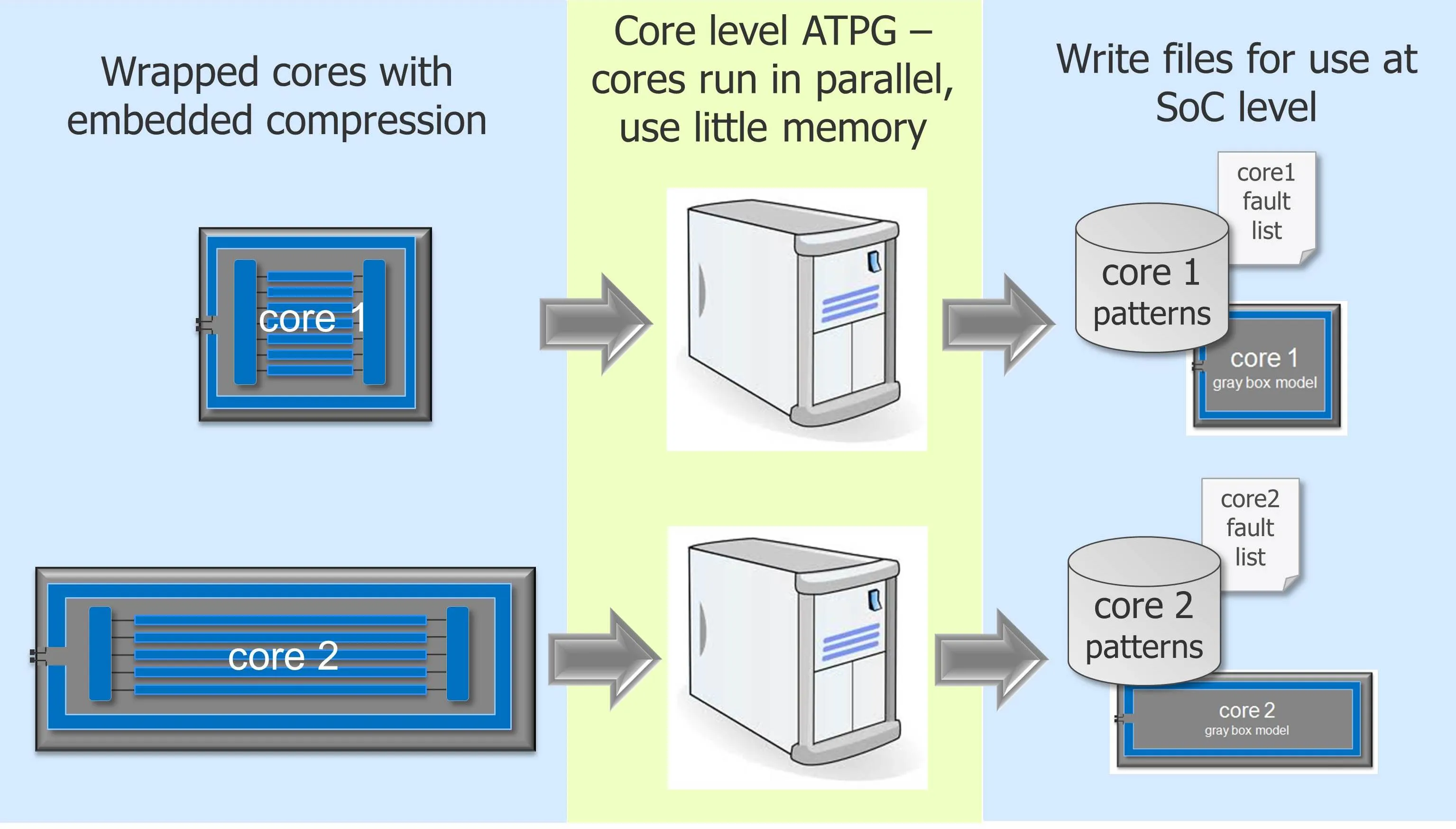
With chips containing billions of transistors, testing the entire design at once is impractical. Hierarchical DFT breaks the design into smaller, manageable blocks, allowing for parallel testing. This technique reduces test data volume by up to 50% and shortens test time significantly, often from days to hours, depending on the design size.
2. Power-Aware DFT
Power consumption during testing can exceed operational limits, risking chip damage. Power-aware DFT techniques, such as low-power test pattern generation, ensure that test power stays within safe limits (e.g., below 80% of peak operational power). This is crucial for battery-powered IoT devices and mobile processors.
3. At-Speed Testing for Timing Faults
Modern high-speed designs, like those for 5G applications, require testing at operational speeds to detect timing-related defects. At-speed testing, often implemented through Built-In Self-Test (BIST) structures, ensures signal integrity at frequencies exceeding 3 GHz in many 2025 designs.
Modern DFT Tools: Driving Efficiency and Precision
The right tools can make or break your DFT strategy. In 2025, modern DFT tools leverage automation, machine learning, and cloud integration to streamline workflows. Here’s a look at the capabilities shaping the industry:
1. Automated DFT Insertion
Manual insertion of test structures is no longer feasible for complex designs. Automated DFT insertion tools integrate scan chains, test points, and BIST logic during the design phase, reducing human error and cutting implementation time by up to 30%.
2. AI-Powered Fault Analysis
Artificial intelligence is transforming DFT by predicting potential fault locations based on design data. AI-driven tools analyze historical test results to prioritize critical areas, improving fault coverage by as much as 15% compared to traditional methods.
3. Cloud-Based Test Simulation
Cloud platforms enable engineers to run massive test simulations without investing in expensive on-site hardware. These tools support parallel processing, slashing simulation times for large designs from weeks to days, even for test sets with over 10 million patterns.
Automation in DFT: The Future of Testing
Automation is at the heart of efficient DFT workflows in 2025. By minimizing manual intervention, automation boosts accuracy and scalability. Here’s how it’s transforming the field:
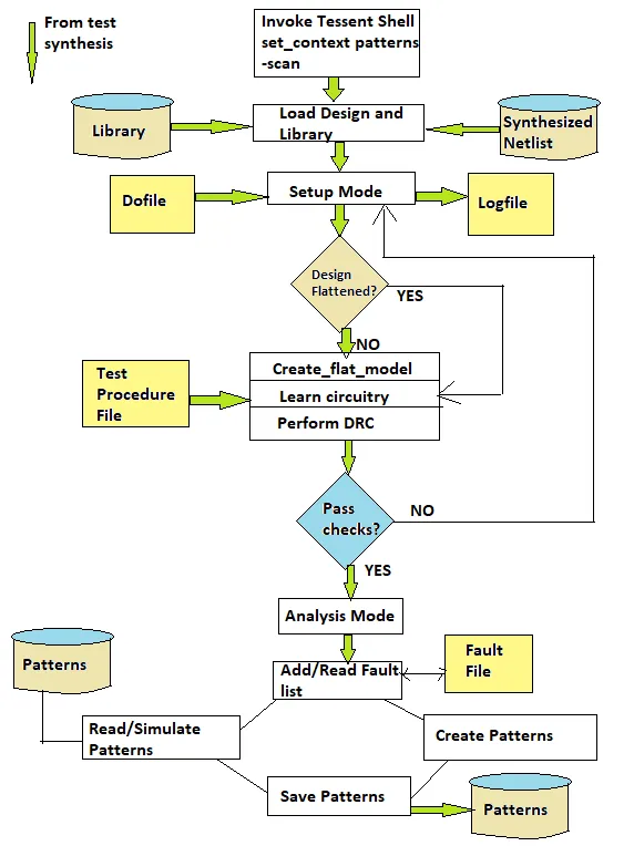
1. Automated Test Pattern Generation (ATPG)
Test pattern generation, or ATPG, is a critical step in DFT. Automated ATPG tools create test vectors to detect stuck-at faults, transition faults, and bridging faults. In 2025, these tools achieve fault coverage rates of over 95% for most designs, even in densely packed ICs with gate counts exceeding 100 million.
2. Scripted Test Flow Integration
Automation scripts integrate DFT processes into the broader design flow, from synthesis to place-and-route. This seamless integration reduces design iterations by up to 20%, ensuring faster time-to-market for new products.
3. Real-Time Test Monitoring
Automated monitoring systems provide real-time feedback during testing, flagging issues like excessive power draw or signal delays (e.g., delays beyond 100 picoseconds in high-speed designs). This allows for immediate adjustments, saving hours of debugging.
Test Pattern Generation (ATPG): Maximizing Fault Coverage
Automatic Test Pattern Generation (ATPG) is the backbone of effective DFT, creating patterns to detect manufacturing defects. In 2025, ATPG has evolved to handle the challenges of advanced nodes and heterogeneous designs. Here’s what you need to know:
1. Targeting Complex Fault Models
Beyond traditional stuck-at faults, modern ATPG targets complex fault models like small delay defects and crosstalk. These patterns ensure reliability in high-performance designs, where signal speeds often exceed 5 GHz.
2. Compression Techniques for Test Data
Large designs generate massive test data volumes, often in the range of terabytes. ATPG compression techniques reduce this by up to 90%, making testing more efficient without sacrificing coverage.
3. Integration with BIST
Built-In Self-Test (BIST) structures work alongside ATPG to enable on-chip testing. This combination is especially valuable for automotive and aerospace chips, where post-manufacturing testing must achieve near-100% fault detection.
DFT Best Practices for 2025: Tips for Success
To stay competitive, engineers must adopt DFT best practices tailored to today’s challenges. Here are actionable strategies to optimize your testing process:
1. Start DFT Early in the Design Cycle
Incorporate DFT planning during the architecture phase, not as an afterthought. Early integration reduces redesign costs by up to 25% and ensures test structures align with design goals.
2. Optimize for Test Time and Cost
Use techniques like test data compression and parallel testing to minimize tester time. For instance, parallel testing can cut test duration by 40% for multi-core designs.
3. Leverage Standards Like IEEE 1149.1 (JTAG)
Adopt industry standards like IEEE 1149.1 for boundary scan testing. This ensures compatibility with a wide range of test equipment and simplifies debugging in complex systems.
4. Focus on Fault Coverage Metrics
Aim for fault coverage above 95% for critical applications. Use ATPG tools to generate detailed reports and identify untested areas, addressing gaps before production.
5. Collaborate Across Teams
Ensure close collaboration between design and test teams to align DFT strategies with product requirements. This reduces miscommunication and speeds up issue resolution by up to 30%.

Challenges in DFT for 2025 and How to Overcome Them
Despite advancements, DFT faces significant hurdles in 2025. Here are common challenges and solutions:
1. Managing Test Data Volume
As designs grow, test data can overwhelm storage and processing capabilities. Use compression algorithms and cloud-based solutions to manage data efficiently, reducing storage needs by up to 80%.
2. Balancing Test Coverage and Power
High test coverage often increases power consumption. Implement power-aware DFT techniques to keep power draw below critical thresholds (e.g., 1.2V for low-power designs).
3. Testing Heterogeneous Designs
Modern chips often integrate analog, digital, and RF components. Use mixed-signal DFT approaches and specialized tools to ensure comprehensive testing across all domains.
Conclusion: Elevate Your DFT Strategy in 2025
Mastering Design for Test in 2025 requires a blend of advanced DFT techniques, modern DFT tools, automation, and best practices. From hierarchical testing and power-aware strategies to AI-driven fault analysis and automated ATPG, the tools and methods available today empower engineers to tackle the complexities of modern chip design. By adopting these approaches, you can achieve higher fault coverage, reduce testing costs, and bring reliable products to market faster.
Staying ahead in the electronics industry means embracing innovation in DFT. Whether you're designing for IoT, AI, or 5G, the insights and strategies in this guide will help you build robust, testable designs that stand the test of time. Partner with a trusted manufacturing and assembly provider to bring your vision to life with precision and quality.


