 ALLPCB


In the fast-paced world of electronics, precision and efficiency in printed circuit board (PCB) manufacturing are more critical than ever. If you're wondering what Laser Direct Imaging (LDI) is and how it impacts PCB production, you're in the right place. LDI is an advanced technology that uses a computer-controlled laser beam to directly expose circuit patterns onto a PCB substrate coated with photosensitive material. This method offers unmatched precision, speed, and flexibility compared to traditional photolithography processes. In this blog, we'll dive deep into the details of LDI, its benefits, applications, and why it's a game-changer for modern PCB fabrication.
What Is Laser Direct Imaging (LDI)?
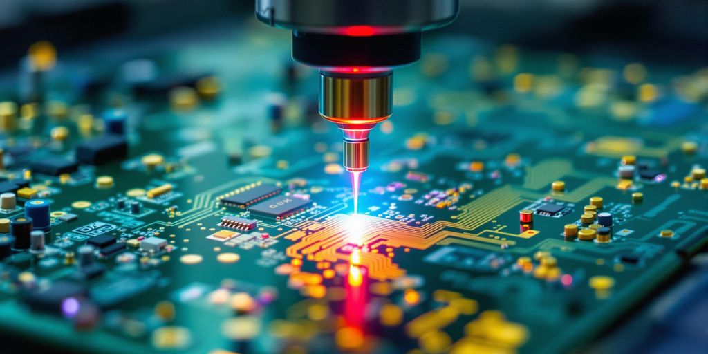
Laser Direct Imaging, commonly referred to as LDI, is a cutting-edge technique used in PCB manufacturing to create highly precise circuit patterns. Unlike traditional methods that rely on photomasks or film negatives to transfer designs onto a board, LDI uses an ultraviolet (UV) laser to directly "write" the circuit pattern onto a photosensitive layer on the PCB. This process is controlled by sophisticated software, ensuring accuracy down to the micrometer level.
The elimination of physical masks not only reduces production time but also minimizes errors caused by misalignment or mask wear. LDI is particularly valuable for high-density interconnect (HDI) boards, flexible circuits, and advanced designs required for 5G technology and IoT devices. By directly imaging the design, manufacturers can achieve finer lines and spaces—often below 50 micrometers—making it ideal for miniaturized electronics.
How Does LDI Work in PCB Manufacturing?
The LDI process is both fascinating and highly efficient. Here's a step-by-step breakdown of how it works:
- Design Data Input: The PCB design is uploaded into the LDI system's software. This digital file contains all the details of the circuit pattern, including traces, pads, and vias.
- Substrate Preparation: The PCB substrate, typically coated with a photosensitive resist material (photoresist), is loaded into the LDI equipment.
- Laser Exposure: A UV laser beam, guided by the digital design data, scans across the photoresist layer. The laser exposes specific areas of the resist, hardening or softening it depending on whether it's a positive or negative photoresist.
- Development: After exposure, the board goes through a chemical development process to remove the unexposed (or exposed, depending on the resist type) areas of the photoresist, revealing the circuit pattern.
- Etching or Plating: The exposed copper areas are either etched away or plated, depending on the manufacturing step, to form the final circuit traces.
This process is incredibly precise, with laser resolutions often reaching 25 micrometers or less. It also allows for real-time adjustments to the design without the need to create new masks, saving both time and cost in production.

Key Advantages of Laser Direct Imaging in PCB Production
LDI technology has transformed PCB manufacturing by offering numerous benefits over traditional methods. Here are some of the standout advantages:
1. Superior Precision for Fine Lines
LDI can achieve line widths and spacing as small as 20-30 micrometers, far surpassing the capabilities of traditional photomask processes, which often struggle below 75 micrometers. This precision is essential for HDI boards used in smartphones, wearables, and medical devices.
2. Elimination of Photomasks
By removing the need for physical masks, LDI reduces costs associated with mask production and storage. It also eliminates errors caused by mask misalignment or degradation over time, ensuring consistent quality across production runs.
3. Faster Turnaround Times
Since LDI directly transfers digital designs to the board, it skips the time-consuming step of creating and aligning masks. This can reduce production lead times by up to 50%, making it ideal for rapid prototyping and high-volume manufacturing.
4. Flexibility for Design Changes
With LDI, design modifications can be made instantly through software updates without the need for new masks. This flexibility is invaluable for iterative design processes, especially in industries where innovation moves quickly.
5. Reduced Material Waste
Traditional methods often result in material waste due to mask errors or misalignments. LDI's digital approach minimizes these issues, making it a more environmentally friendly option for PCB fabrication.
6. Enhanced Quality Control
LDI systems often include built-in inspection tools that verify alignment and exposure accuracy in real time. This leads to fewer defects and higher yields, with some manufacturers reporting defect rates dropping by as much as 30% after adopting LDI.
Applications of LDI in Modern Electronics
The precision and efficiency of LDI make it a preferred choice for a wide range of applications in the electronics industry. Some key areas where LDI shines include:
- High-Density Interconnect (HDI) PCBs: Used in compact devices like smartphones and tablets, HDI boards require microvias and fine traces that LDI can deliver with ease. For example, modern HDI designs often feature via diameters as small as 50 micrometers, which LDI can image accurately.
- Flexible and Rigid-Flex PCBs: LDI's ability to handle complex geometries and thin substrates makes it ideal for flexible circuits used in wearables and automotive applications.
- 5G Technology: The high-frequency signals in 5G devices demand tight impedance control and minimal signal loss. LDI ensures precise trace widths, often within tolerances of ±5 micrometers, to meet these requirements.
- Medical Electronics: Devices like pacemakers and diagnostic equipment rely on miniature, reliable PCBs. LDI enables the production of these intricate designs with high repeatability.

Challenges and Limitations of LDI Technology
While LDI offers significant advantages, it's not without its challenges. Understanding these limitations can help manufacturers make informed decisions about adopting this technology.
1. High Initial Investment
LDI equipment is expensive, often costing hundreds of thousands of dollars. This can be a barrier for smaller manufacturers, though the long-term savings in mask costs and reduced defects often justify the investment.
2. Complexity of Operation
Operating LDI systems requires skilled technicians and specialized software. Training staff and maintaining the equipment can add to operational costs, though automation is helping to reduce this burden.
3. Material Compatibility
Not all photoresist materials are optimized for LDI's UV laser wavelengths, typically around 355-405 nanometers. Manufacturers may need to test and select specific resists to achieve the best results.
Despite these challenges, ongoing advancements in LDI technology are addressing these issues, making it more accessible and efficient for a broader range of manufacturers.
The Future of LDI in PCB Manufacturing
The demand for smaller, faster, and more complex electronics continues to grow, and LDI is poised to play a central role in meeting these needs. According to recent industry reports, the global LDI equipment market is projected to reach $1.73 billion by 2034, growing at a compound annual growth rate (CAGR) of 9.6% from 2025 onward. This growth is driven by the increasing adoption of HDI, 5G, and IoT technologies.
Future developments in LDI are expected to focus on even higher resolution imaging, with some systems targeting line widths below 10 micrometers. Additionally, improvements in laser speed and automation will further reduce production times, while advancements in photoresist materials will enhance compatibility and imaging quality.
Why Choose LDI for Your PCB Projects?
For engineers and manufacturers, the decision to use LDI comes down to the need for precision, speed, and reliability. Whether you're working on a prototype for a cutting-edge wearable device or mass-producing boards for automotive systems, LDI can help you achieve superior results. Its ability to handle fine traces, reduce defects, and adapt to design changes makes it a powerful tool in today's competitive electronics market.
At ALLPCB, we understand the importance of staying ahead with the latest manufacturing technologies. By incorporating LDI into our processes, we ensure that our customers receive high-quality PCBs that meet the strictest standards of accuracy and performance. If you're looking to elevate your PCB designs with the benefits of Laser Direct Imaging, we're here to support you every step of the way.
Conclusion
Laser Direct Imaging (LDI) is more than just a trend—it's a transformative technology that’s reshaping the landscape of PCB manufacturing. With its unparalleled precision, faster production times, and flexibility for complex designs, LDI is the go-to choice for modern electronics, from HDI boards to 5G applications. While the initial costs and technical requirements may pose challenges, the long-term benefits of reduced defects, lower waste, and improved quality make it a worthwhile investment for many manufacturers.
As the electronics industry continues to evolve, LDI will remain at the forefront, driving innovation and enabling the creation of smaller, smarter, and more efficient devices. For anyone involved in PCB design or production, understanding and leveraging LDI technology is key to staying competitive in this dynamic field.


