ALLPCB


Choosing the right type of printed circuit board (PCB) for your project can make or break its success. If you're wondering whether a double-layer PCB is the best fit, you're in the right place. In short, a double-layer PCB is ideal for projects with moderate complexity, requiring more routing space than a single-layer board but not the advanced capabilities of multilayer designs. This guide will dive deep into the specifics of double-layer PCBs, compare them with multilayer options, and walk you through key PCB design considerations and project requirements to help you make an informed decision.
Whether you're an engineer working on a consumer electronics prototype or a designer tackling an industrial application, this PCB selection guide will provide actionable insights. Let’s explore the world of double-layer PCBs and see if they match your needs.
What Is a Double-Layer PCB and How Does It Work?
A double-layer PCB, also known as a two-layer or double-sided PCB, consists of two conductive layers of copper, typically separated by an insulating substrate material like FR-4. These layers are connected through vias—small holes filled or plated with conductive material that allow electrical signals to pass between the top and bottom layers. This design offers more space for routing traces compared to a single-layer PCB, making it suitable for moderately complex circuits.
Double-layer PCBs are widely used in applications like power supplies, LED lighting systems, and basic consumer electronics. Their ability to handle more components and connections than single-layer boards while remaining cost-effective makes them a popular choice for many projects. For instance, a simple audio amplifier circuit might fit perfectly on a double-layer PCB, with power and ground traces on one layer and signal traces on the other, reducing interference.

Double-Layer PCB vs. Multilayer PCB: Key Differences
One of the most common dilemmas in PCB selection is deciding between a double-layer PCB or multilayer design. Understanding their differences is crucial for matching the board to your project requirements.
- Layer Count and Complexity: A double-layer PCB has two conductive layers, while multilayer PCBs have three or more (often 4, 6, or even 16 layers). Multilayer boards are designed for high-density, complex circuits, such as those in smartphones or medical devices, where space is limited, and signal integrity is critical.
- Cost: Double-layer PCBs are more affordable due to simpler manufacturing processes. For example, a double-layer board might cost around 30-50% less per unit than a 4-layer board for the same dimensions, depending on volume and specifications.
- Signal Integrity: Multilayer PCBs offer better control over signal integrity by allowing dedicated ground and power planes. This reduces noise and electromagnetic interference (EMI), which is vital for high-speed circuits operating above 100 MHz. Double-layer PCBs can struggle with EMI in such scenarios unless carefully designed.
- Size and Space: Multilayer boards can pack more functionality into a smaller footprint by stacking layers vertically. A double-layer PCB might require a larger board area to accommodate the same number of components and traces.
For a project like a basic microcontroller-based sensor system, a double-layer PCB is often sufficient. However, if you're designing a high-speed communication device with multiple signal paths, a multilayer PCB becomes necessary to maintain performance.

Advantages and Limitations of Double-Layer PCBs
Before committing to a double-layer PCB, it’s important to weigh its benefits and drawbacks in the context of your project needs.
Advantages
- Cost-Effective: Double-layer PCBs strike a balance between functionality and price, making them ideal for small to medium-scale production runs.
- Moderate Complexity: They support more components and routing options than single-layer boards, suitable for designs with up to a few hundred connections.
- Easier to Design: Compared to multilayer boards, double-layer PCBs are simpler to layout and troubleshoot, especially for engineers new to PCB design.
Limitations
- Limited Routing Space: With only two layers, routing dense or high-speed circuits can become challenging, often leading to crosstalk or signal delays.
- Signal Integrity Issues: Without dedicated ground planes, maintaining low impedance for high-frequency signals (above 50 MHz) can be difficult.
- Not Ideal for Compact Designs: If your project demands a very small form factor, a multilayer PCB might be a better choice to stack components vertically.
Understanding these trade-offs is key to deciding if a double-layer PCB aligns with your project goals. For example, a hobbyist building a simple LED control circuit will find a double-layer board more than adequate, while a professional designing a high-speed data logger might face limitations.
PCB Design Considerations for Double-Layer Boards
Designing a double-layer PCB requires careful planning to ensure functionality, reliability, and manufacturability. Below are critical PCB design considerations to keep in mind.
1. Component Placement and Routing
Place components logically to minimize trace lengths and avoid crossing signals. Group related components together—for instance, keep power supply components near the input connector to reduce noise. On a double-layer PCB, use one layer primarily for horizontal traces and the other for vertical traces to simplify routing and reduce vias.
2. Grounding and Power Distribution
Since double-layer PCBs lack dedicated ground planes, create a ground grid or use wide traces to minimize impedance. For a circuit with a 5V power supply, ensure power traces are at least 20-30 mils wide to handle currents up to 1A without significant voltage drops (based on standard PCB trace width calculators).
3. Signal Integrity
For signals operating at frequencies above 10 MHz, pay attention to trace impedance and spacing. Keep high-speed signal traces short and avoid running them parallel to power lines to prevent crosstalk. If your design includes analog and digital signals, separate them on different layers to reduce interference.
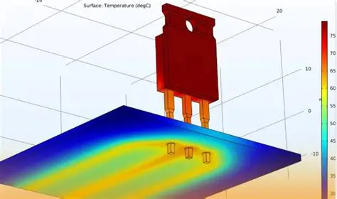
4. Thermal Management
Double-layer PCBs can struggle with heat dissipation in high-power applications. Use copper pours or thermal vias to spread heat from power components like voltage regulators. For a component dissipating 2W of heat, a copper area of at least 1 square inch can help maintain safe operating temperatures.
5. Manufacturability
Stick to standard design rules, such as minimum trace widths (typically 6-8 mils) and spacing, to ensure your board can be fabricated without issues. Check with your manufacturing partner for specific guidelines on via sizes and drill tolerances.

Project Requirements: When to Choose a Double-Layer PCB
Your project requirements play a pivotal role in determining whether a double-layer PCB is the right choice. Consider the following factors as part of your PCB selection guide.
1. Circuit Complexity
If your circuit has fewer than 100-200 components or connections, a double-layer PCB is often sufficient. For instance, a basic motor control circuit with a microcontroller, a few sensors, and drivers can easily fit on two layers.
2. Budget Constraints
For cost-sensitive projects, double-layer PCBs offer a practical solution. They are significantly cheaper than multilayer boards, especially for prototypes or low-volume production. A typical 100mm x 100mm double-layer board might cost around $1-2 per unit in small batches, compared to $3-5 for a 4-layer board.
3. Performance Needs
Evaluate the speed and performance requirements of your circuit. If your design operates at low to medium frequencies (below 50 MHz) and doesn’t require strict signal isolation, a double-layer PCB can work well. However, for high-speed applications like RF circuits, multilayer boards with controlled impedance layers are better suited.
4. Size and Form Factor
If your project allows for a larger board size, a double-layer PCB can accommodate the necessary traces and components without needing additional layers. This is common in industrial control systems where space isn’t a primary concern.
5. Production Volume and Timeline
Double-layer PCBs are quicker to manufacture and test, which can be advantageous for projects with tight deadlines or iterative prototyping phases. Their simpler structure also reduces the risk of manufacturing defects compared to multilayer designs.
Tips for Optimizing Your Double-Layer PCB Design
To get the most out of a double-layer PCB, follow these practical tips during the design phase.
- Plan Vias Carefully: Minimize the number of vias to reduce manufacturing costs and potential failure points. Place vias away from high-stress areas of the board.
- Use Design Software: Leverage PCB design tools to simulate signal paths and check for errors before fabrication. Many software options offer layer-specific views to help with routing.
- Test Iteratively: Build and test prototypes to identify issues like noise or thermal hotspots early in the development process.
- Consult Experts: If you’re unsure about specific design aspects, collaborate with experienced engineers or manufacturing partners to refine your layout.
Common Applications of Double-Layer PCBs
Double-layer PCBs are versatile and used across various industries. Some common applications include:
- Consumer Electronics: Devices like remote controls, calculators, and basic audio equipment often use double-layer PCBs for their balance of cost and functionality.
- Automotive Systems: Simple control modules, such as those for interior lighting or window controls, can be built on two-layer boards.
- Industrial Equipment: Sensors, timers, and basic automation controllers frequently rely on double-layer PCBs due to their reliability and affordability.

Conclusion: Making the Right Choice for Your Project
Deciding whether a double-layer PCB is right for your project comes down to balancing complexity, cost, and performance needs. As a PCB selection guide, this article has walked you through the essentials of double-layer PCBs, compared them to multilayer options, and highlighted critical PCB design considerations and project requirements.
For many engineers and designers, double-layer PCBs offer a sweet spot—providing enough routing space for moderate designs while keeping costs low. If your project involves basic to intermediate circuits, operates at lower frequencies, and fits within a reasonable board size, a double-layer PCB is likely the perfect choice. However, for high-speed, compact, or highly complex designs, exploring multilayer options might be necessary.
By carefully evaluating your needs and following best practices in design, you can ensure your PCB supports your project’s goals. With the insights from this decision-making guide, you’re well-equipped to choose the right board and bring your electronic designs to life with confidence.