ALLPCB


Integrated circuit (IC) design is divided into front-end design (logical design) and back-end design (physical design). While not strictly separated, back-end design typically involves process-related tasks. Below is an overview of the key steps and tools used in each phase.
Front-End Design Flow
1. Specification Definition
The process begins with defining the chip's specifications, outlining the required functions and performance metrics based on customer requirements provided to fabless design companies.
2. Detailed Design
Designers develop a solution and architecture, breaking down the chip into functional modules based on the specifications.
3. HDL Coding
Module functions are described using hardware description languages (HDL), primarily Verilog HDL, to create register-transfer level (RTL) code representing hardware behavior.
Tools:
- Language Input: Summit VisualHDL, Mentor Renoir
- Graphical Input: Cadence Composer, Viewlogic Viewdraw
4. Simulation and Verification
Simulation verifies the design's correctness against the specifications. This iterative process, known as pre-simulation (functional, behavioral, or logical simulation), ensures compliance with requirements. Post-layout simulation (timing simulation) follows later.
Tools for Verilog HDL:
- Mentor Modelsim
- Synopsys VCS
- Cadence NC-Verilog, Verilog-XL
Tools for VHDL:
- Mentor Modelsim
- Synopsys VSS
- Cadence NC-VHDL, Leapfrog
5. Logic Synthesis
After verification, HDL code is translated into a gate-level netlist using logic synthesis, constrained by area and timing goals. The choice of synthesis library affects the circuit's timing and area due to variations in standard cell parameters.
Tools:
- Synopsys Design Compiler, Behavioral Compiler, DC-Expert
- Cadence Buildgates, Envisia Ambit
- Mentor Leonardo
6. Static Timing Analysis (STA)
STA verifies timing, checking for setup and hold time violations that could prevent accurate data sampling in registers, ensuring reliable chip functionality.
Tools:
- Synopsys PrimeTime
- Cadence Pearl, Tempus
- Mentor SST Velocity
7. Formal Verification
Formal verification ensures the synthesized netlist functionally matches the verified HDL design, typically through equivalence checking, confirming that logic synthesis preserved the original functionality.
Tools:
- Synopsys Formality
- Cadence LEC, FormalCheck
- Mentor FormalPro
The front-end design concludes with a gate-level netlist.
Back-End Design Flow
1. Design for Test (DFT)
DFT incorporates test circuits, such as scan chains, to enhance testability by converting non-scannable units (e.g., registers) into scannable ones.
Tools:
- BSCAN (IO Pad Testing): Mentor BSDArchitect, Synopsys BSD Compiler
- MBIST (Memory Testing): Mentor MBISTArchitect, Tessent MBIST
- ATPG (Standard Logic Testing): Mentor TestKompress, Synopsys TetraMAX (ATPG generation), Synopsys DFT Compiler (scan chain insertion)
2. Floorplanning
Floorplanning positions macro cells, IP modules, RAM, and I/O pins, determining the chip's layout and directly impacting its final area.
Tools:
- Synopsys Astro, Physical Compiler, IC Compiler
- Cadence Encounter, PKS, Silicon Ensemble, Design Planner
3. Clock Tree Synthesis (CTS)
CTS routes the clock signal symmetrically to registers, minimizing skew and ensuring uniform delay from the clock source, critical for synchronous designs.
Tools:
- Synopsys Clock Tree Compiler
- Cadence CT-Gen
4. Place and Route
Place and route transforms the netlist into a physical layout, connecting standard cells (logic gates) with metal wires. Process nodes (e.g., 0.13¦Ìm, 90nm) refer to the minimum wire width or MOS transistor channel length.
Tools:
- Synopsys Astro, Physical Compiler, IC Compiler
- Cadence Encounter, PKS, Silicon Ensemble, Design Planner
5. Parasitic Extraction
Parasitic effects (resistance, inductance, capacitance) cause noise, crosstalk, and reflections, impacting signal integrity. Extracting and analyzing parasitics is crucial to prevent signal distortion.
Tools:
- Synopsys Star-RCXT
- Mentor Calibre xRC
- Cadence Assura RCX
6. Physical Verification
Physical verification ensures the layout meets functional and timing requirements, including:
- LVS (Layout vs. Schematic): Compares the layout to the gate-level netlist.
- DRC (Design Rule Checking): Verifies wire spacing and width against process rules.
Tools:
- Synopsys Hercules
- Cadence Dracula, Diva, Assura
- Mentor Calibre
Post-simulation (timing simulation) accounts for actual delays, using the same tools as pre-simulation. Additional steps like power analysis and design for manufacturability (DFM) may follow.
Conclusion
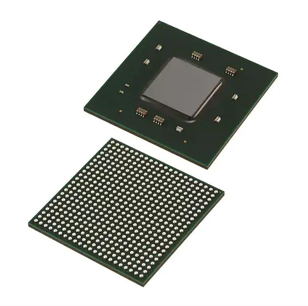
After physical verification, the chip design is complete. The layout, formatted as GDSII, is sent to a foundry for fabrication on silicon wafers, followed by packaging and testing to produce the final chip.