 ALLPCB


Designing an impedance matching network on a PCB using lumped components is a critical skill for engineers working on high-frequency or high-speed circuits. Whether you're ensuring signal integrity or optimizing power transfer, a well-designed PCB impedance matching network can make all the difference. In this comprehensive guide, we’ll walk you through the step-by-step process of designing such a network using lumped elements like capacitors, inductors, and resistors. By the end, you’ll have a clear understanding of how to use tools like an impedance matching calculator and apply a practical PCB impedance matching guide to your projects.
What Is an Impedance Matching Network and Why Is It Important?
An impedance matching network is a circuit designed to match the impedance of a source to that of a load. On a PCB, this is often necessary for high-frequency signals, such as those in RF (radio frequency) or high-speed digital designs. When impedances are mismatched, signal reflections occur, leading to power loss, noise, or even data errors. Using a lumped element matching network—which relies on discrete components like surface-mount technology (SMT component impedance matching)—is a common and effective approach for many PCB designs.
The primary goals of impedance matching are to maximize power transfer and minimize signal distortion. For example, in an RF circuit operating at 2.4 GHz, a mismatched impedance could result in a significant loss of signal strength. By designing a proper matching network, you ensure that your circuit performs efficiently, whether it’s for a wireless communication device or a high-speed data interface.
Understanding the Basics of Lumped Components in Impedance Matching
Lumped components are discrete elements like capacitors, inductors, and resistors that are small enough to be considered "lumped" at the frequencies of interest. This means their physical size is much smaller than the wavelength of the signal, allowing us to ignore distributed effects like transmission line behavior. These components are ideal for PCB designs because they are compact, widely available in SMT packages, and easy to integrate.
In a lumped element matching network, capacitors and inductors are typically arranged in specific configurations (like L, Pi, or T networks) to adjust the impedance. Resistors may also be used to dampen unwanted oscillations or to handle specific matching scenarios. The choice of components depends on the frequency range, the impedance values of the source and load, and the desired bandwidth of the match.
Key Steps to Design a PCB Impedance Matching Network
Designing a PCB impedance matching network involves a systematic approach. Below, we break down the process into actionable steps to help you achieve optimal results using lumped components.
Step 1: Determine the Source and Load Impedances
The first step is to identify the impedance of your source and load. For instance, a common RF source might have an impedance of 50 ohms, while an antenna (the load) might have a complex impedance of 30 + j20 ohms at a specific frequency. You can measure these values using a network analyzer or refer to component datasheets. Knowing these values is crucial because the matching network will transform the load impedance to match the source, ensuring maximum power transfer.
Step 2: Choose the Operating Frequency and Bandwidth
Next, define the frequency or range of frequencies at which your circuit will operate. Lumped components behave differently at various frequencies due to parasitic effects like stray capacitance or inductance. For example, at frequencies above 1 GHz, parasitic effects in SMT components can significantly alter their performance. Additionally, decide on the bandwidth over which the match should be effective. A narrowband design might suffice for a single-frequency application, while a broadband design may require more complex networks.
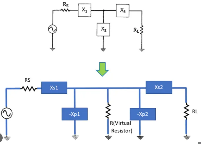
Step 3: Select a Matching Network Topology
There are several common topologies for a lumped element matching network, including:
- L-Network: Uses two components (e.g., a capacitor and an inductor) and is simple but limited to specific impedance transformations.
- Pi-Network: Uses three components and offers more flexibility for broadband matching.
- T-Network: Similar to the Pi-network, it’s useful for specific impedance ranges and bandwidths.
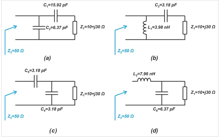
The L-network is often the starting point due to its simplicity and minimal component count, which saves board space on a PCB. For instance, if you’re matching a 50-ohm source to a 100-ohm load at 100 MHz, an L-network with a series inductor of 79.6 nH and a shunt capacitor of 31.8 pF might work (values calculated using standard formulas).
Step 4: Calculate Component Values Using an Impedance Matching Calculator
Calculating the exact values of lumped components can be complex, especially for multi-component networks. This is where an impedance matching calculator becomes invaluable. These tools allow you to input source and load impedances, operating frequency, and desired topology, then output the required component values. Many online calculators are available, or you can use simulation software with built-in matching tools.
For example, to match a 50-ohm source to a 75-ohm load at 500 MHz using an L-network, a calculator might suggest a series inductor of 23.9 nH and a shunt capacitor of 21.2 pF. Always double-check these values with simulation or manual calculations to account for real-world component tolerances and parasitics.
Step 5: Select SMT Components for the Matching Network
Once you have the calculated values, choose appropriate SMT component impedance matching parts. Look for components with tight tolerances (e.g., ±5% for capacitors and inductors) and low parasitic effects. Check the self-resonant frequency (SRF) of inductors and capacitors to ensure they operate effectively at your design frequency. For instance, a capacitor with an SRF of 800 MHz is unsuitable for a 1 GHz design because it will behave more like an inductor at that frequency.
Also, consider the power handling and voltage ratings of the components, especially in RF applications where high power levels might be present. Place these components as close as possible to the source and load on the PCB to minimize trace inductance.
Step 6: Simulate and Optimize the Design
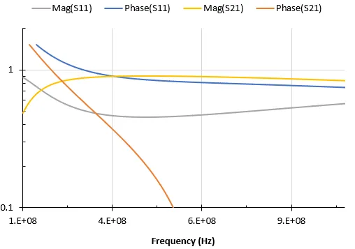
Before finalizing your design, simulate the matching network using circuit simulation software. This step helps identify issues like parasitic effects or mismatches that weren’t accounted for in initial calculations. Adjust component values if necessary to fine-tune the match. For example, if a simulation shows a return loss of only -10 dB (indicating poor matching), you might need to tweak the inductor or capacitor values slightly.
Step 7: Layout Considerations on the PCB
The physical layout of your PCB impedance matching network is just as important as the component selection. Poor layout can introduce unwanted inductance or capacitance, ruining the match. Follow these best practices:
- Keep traces as short as possible to reduce parasitic inductance.
- Use a solid ground plane beneath the matching network to minimize interference.
- Avoid sharp corners in traces; use 45-degree bends or curves to maintain signal integrity.
- Place components close to the source and load to reduce transmission line effects.
For high-frequency designs, ensure that the PCB material has a suitable dielectric constant (e.g., FR-4 with a dielectric constant of 4.2-4.6 is common for frequencies up to a few GHz). If higher frequencies are involved, consider low-loss materials like Rogers laminates.
Common Challenges and How to Overcome Them
Designing a matching network isn’t without challenges. Here are some common issues and tips to address them:
- Component Tolerances: Real-world components have tolerances that can affect the match. Use components with tight tolerances or simulate worst-case scenarios to ensure performance.
- Parasitic Effects: At high frequencies, parasitics can dominate. Always check the SRF and equivalent series resistance (ESR) of components, and account for them in simulations.
- Bandwidth Limitations: Simple networks like the L-network have narrow bandwidths. For broader bandwidths, consider Pi or T networks, though they require more components and board space.
Tools and Resources for PCB Impedance Matching
To make the design process easier, leverage available tools and resources. Online impedance matching calculators can quickly provide component values for common topologies. Additionally, simulation software allows you to model the entire circuit, including PCB parasitics, for more accurate results. Many design platforms also offer built-in tools for impedance control and matching network design, streamlining the process.
Final Tips for a Successful PCB Impedance Matching Design
As you embark on designing your PCB impedance matching network, keep these final tips in mind:
- Always start with accurate measurements of source and load impedances.
- Validate your design through simulation before committing to a physical prototype.
- Pay close attention to PCB layout to avoid introducing unwanted effects.
- Test the final design with real hardware to confirm performance, using tools like a vector network analyzer to measure return loss and insertion loss.
By following this PCB impedance matching guide and using lumped components effectively, you can ensure your circuits operate with optimal signal integrity and efficiency. Whether you’re working on RF systems, high-speed digital interfaces, or other applications, mastering impedance matching is a valuable skill that enhances the reliability of your designs.
Conclusion
Designing an impedance matching network on a PCB using lumped components doesn’t have to be daunting. By understanding the basics of SMT component impedance matching, choosing the right topology, calculating component values with an impedance matching calculator, and optimizing your PCB layout, you can achieve excellent results. This process ensures minimal signal loss and maximum power transfer, which are crucial for high-performance circuits. With the steps and tips provided in this guide, you’re well-equipped to tackle your next PCB design project with confidence.


