ALLPCB


Overview
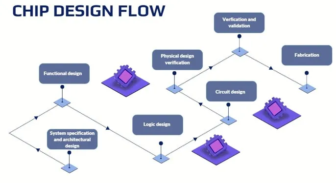
Chip development has been a major focus in recent years, and many established companies pursue in-house chip projects. That has created many roles. Compared with hardware engineers, software developers have a narrower scope of tasks but play important roles. Software typically participates in requirements, architecture, and verification. This article outlines the basic chip design flow from the author’s experience and highlights several frequently mentioned technical chokepoints.
This article focuses on the requirements and design stages; fabrication and packaging are handled by other teams and suppliers.
1. Market Demand
To develop a chip there must be demand, i.e., an application scenario with customers. In the current technology era, electronic technology is widely applied; wherever there is a printed circuit board there is potential chip demand, for example in phones, computers, and smart appliances.
With a defined demand, teams derive the required hardware modules, performance targets, and supporting software and hardware technologies. Architects design the system architecture and produce a specification document. The spec defines all functions and requirements and is the basis for subsequent chip design.
1.1 EDA and Emulation Tools
During architecture design, software validation can be performed with emulation such as QEMU to check whether applications run. IC vendors often provide IP integration tools to model the SoC purely in software, for example VDK (Virtualizer Development Kit). VDK is a type of electronic design automation (EDA) tool. EDA is a complex and critical technology that spans design, verification, and manufacturing. Verification in particular reduces error costs and shortens development cycles.
QEMU supports a limited set of chip models and extending it requires source changes. A tool like VDK provides a graphical interface to add IP models more easily. Many IPs are vendor-private and not broadly supported, so IP vendors typically supply integration and verification tools for customers.
Chip development cycles are long. Early in the requirements stage, some software can already be developed on QEMU or VDK. Applications that depend on SoC IPs can be exercised at the data-flow level before business logic is supported on silicon. Early software work reduces subsequent integration tasks and allows early validation of software approaches. If a software approach is infeasible, the SoC can be adjusted early; late-stage hardware changes are far more expensive and risky, especially after tape-out.
1.2 About Architects
Digital integrated circuit design is a lengthy process. For example, mobile baseband engineers work from extensive protocol documents for 3G, 4G, and 5G. The architecture and implementation roles are generally:
- Architects determine which protocol portions are implemented in software and which in hardware.
- Algorithm engineers study protocols and choose implementation algorithms.
- Design engineers translate algorithms into RTL.
- Verification engineers create test vectors and verify RTL functionality and performance.
- Digital implementation engineers convert RTL into GDS according to PPA (power, performance, area) targets.
- Foundries handle fabrication and packaging; most companies rent third-party test equipment for production testing.
Architects define the high-level structure and requirements used by the rest of the team.
2. Chip Design Overview
Chip design is divided into front-end (logical design) and back-end (physical design).
Many steps appear complex, but with vendor-provided IP and tools much work is performed through graphical interfaces. Most commercial EDA tools and flows originate from non-local vendors, which affects tool availability and costs in different markets. Some vendors offer closed-source, commercial tools; local suppliers may distribute vendor tools more quickly to nearby customers, sometimes resulting in rapid local adoption or reimplementation.
3. Front-End Design
- RTL design
- Verification
- Static timing analysis
- Coverage
- ASIC logic synthesis
3.1 RTL Design
First the target process node is chosen.
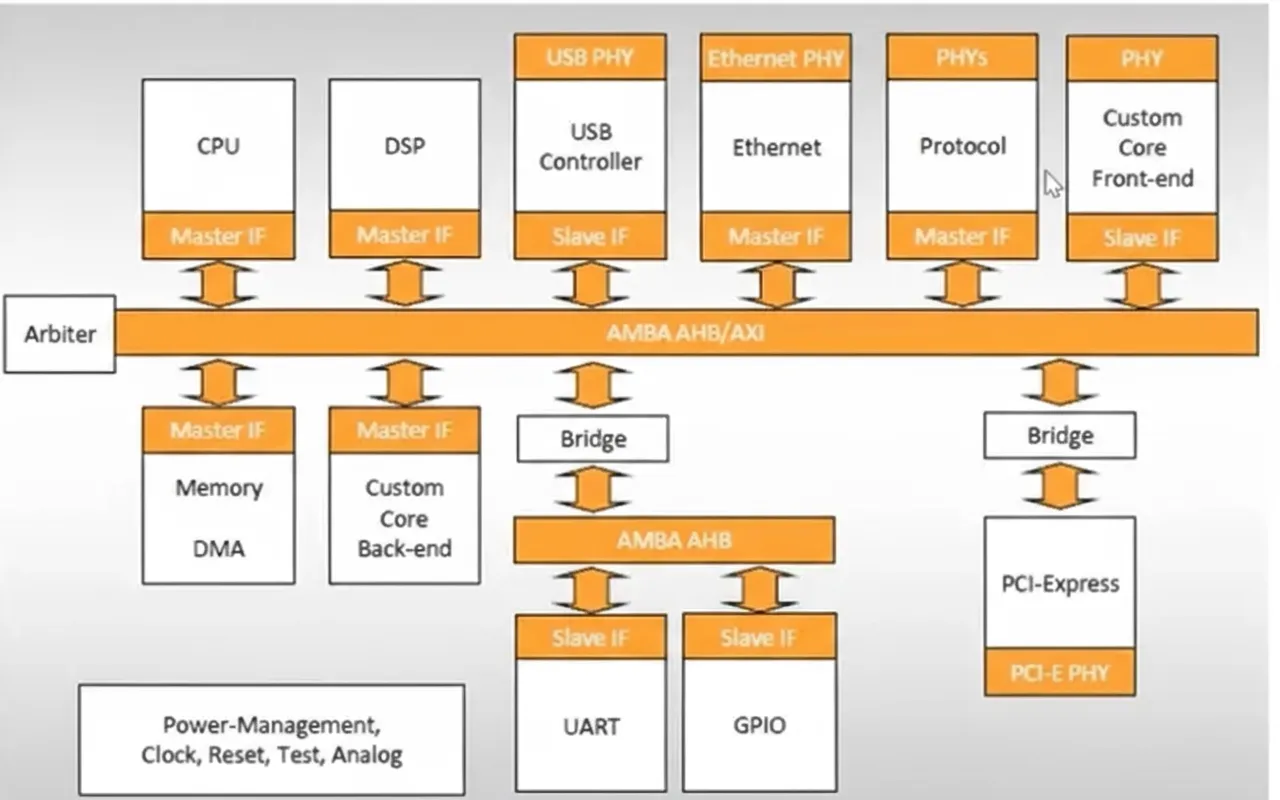
RTL (register transfer level) design uses hardware description languages such as VHDL, Verilog, and SystemVerilog to describe data transfers between registers. RTL code implements functional modules, i.e., IP blocks. IPs are categorized as digital IP and analog IP.
SoC integration engineers combine IP blocks into a complete SoC. A typical SoC contains IPs such as CPU, DSP, USB peripherals, and memory. RTL design also includes support for built-in self-test (BIST) and design-for-test (DFT).
Static code checks are run with tools such as lint and Spyglass to enforce design rules, coding style, DFT practices, naming conventions, and synthesis-related checks.
3.2 Verification
Verification is the most important stage for ensuring correctness and completeness. Verification typically occupies 50%–70% of the development schedule; verification engineers usually outnumber design engineers by about 2–3:1. Verification levels include module, subsystem, and system. Verification approaches include simulation and formality checks.
Software developers are involved again here. Code exercised on QEMU and VDK can be run on RTL simulations, getting closer to the hardware. Cross-platform verification is repetitive but valuable. Code reuse across verification platforms is important: large platform differences can be handled at compile time, small differences by runtime flags or configuration files. Practical suggestion: prefer configuration files such as XML, DTS, or plain config files; avoid excessive conditional macros; use debug builds adaptable to multiple verification platforms and use build scripts to automate compile-time selection.
3.3 Static Timing Analysis (STA)
Static timing analysis applies timing models to a design to verify whether timing constraints are met. The mainstream STA tool is Synopsys PrimeTime.
STA purposes:
- Determine the maximum operating frequency of the chip.
- Guide synthesis, mapping, placement, and routing to reduce delay and improve frequency.
- Check whether timing constraints are satisfied.
- Locate timing violations and provide specific reasons for corrective action.
- Analyze clock quality, including jitter, skew, and duty-cycle distortion, and their impact on target modules.
3.4 Coverage
Coverage is a primary measure of verification completeness. Coverage targets are typically split into code coverage and functional coverage:
- Code coverage checks for untested or redundant RTL code.
- Functional coverage checks whether specified features and scenarios have been exercised using custom coverage containers.
At sign-off, teams must justify any coverage shortfalls to ensure no functional risk remains for the silicon.
3.5 ASIC Synthesis
Logic synthesis translates RTL into a gate-level netlist. Synthesis requires constraints such as area and timing targets. A common tool is Synopsys Design Compiler. The resulting netlist is passed to the back-end team.
With synthesis complete, front-end work is essentially finished.
4. Back-End Design
- Logic synthesis
- Formality verification
- Physical implementation
- Clock tree synthesis (CTS)
- Parasitic extraction
- Layout physical verification
4.1 Logic Synthesis
See section 3.5 for the front-end synthesis process.
4.2 Formality Verification
- Verify functional consistency between stages.
- Do not verify analog circuit correctness.
- Run after any design change.
Formality verification ensures consistency between RTL and synthesized netlists. It is typically performed after synthesis and place-and-route. A common tool is Synopsys Formality.
4.3 Physical Implementation
Physical implementation comprises:
- Floorplanning
- Placement
- Routing
Floorplanning is a flexible but critical step that balances many tradeoffs. The goals of placement and routing are to optimize chip area, achieve timing closure, and maintain routability. Typical tools include IC Compiler and Encounter. Floorplan visualization is important for evaluating tradeoffs.
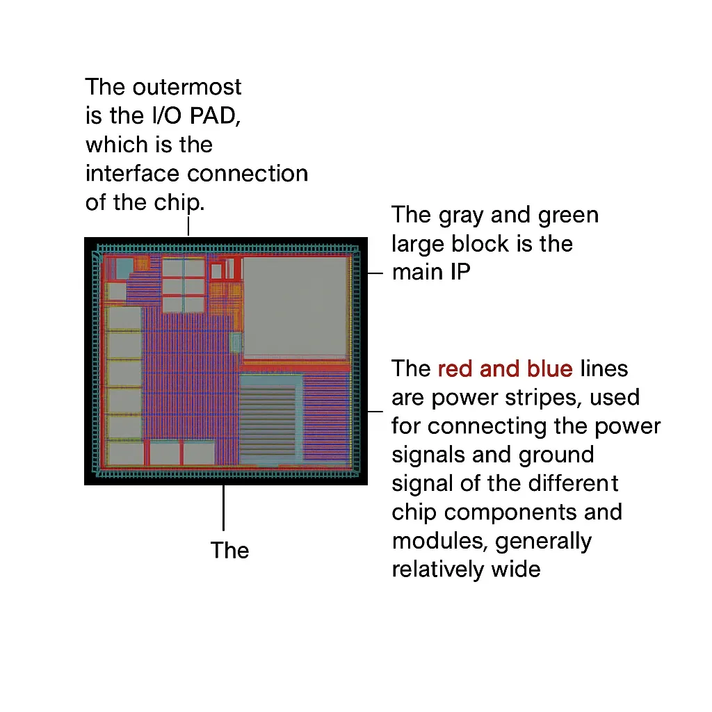
Placement arranges standard cells, I/O pads, and macros to realize the circuit logic. Placement goals are high utilization, short interconnects, and favorable timing; these goals often conflict and require compromise.
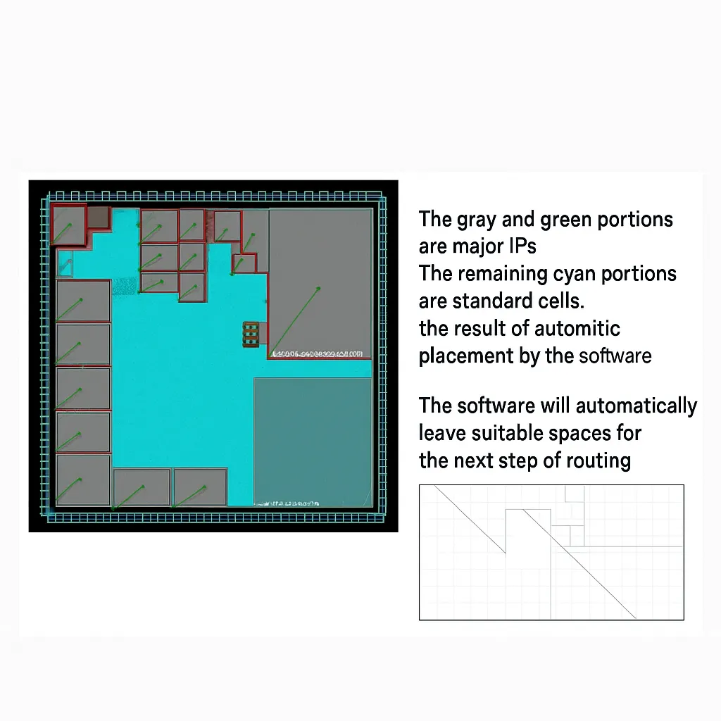
Routing connects cells and I/O pads under design-rule and electrical constraints such as layer limits, wire width, and spacing requirements.
4.4 Clock Tree Synthesis (CTS)
CTS is the routing and buffering of clock signals. Because the clock is a global control signal, its distribution should be balanced so that clock arrival times at registers have minimal skew. That is why clocks often use dedicated routing and special handling.
4.5 Parasitic Extraction
Wires exhibit resistance, and adjacent wires couple via capacitance. These parasitic effects cause noise, crosstalk, and reflections that can degrade signal integrity. Extracting parasitic parameters and reanalyzing the design is important to identify and fix signal integrity issues. A common tool is Synopsys Star-RCXT.
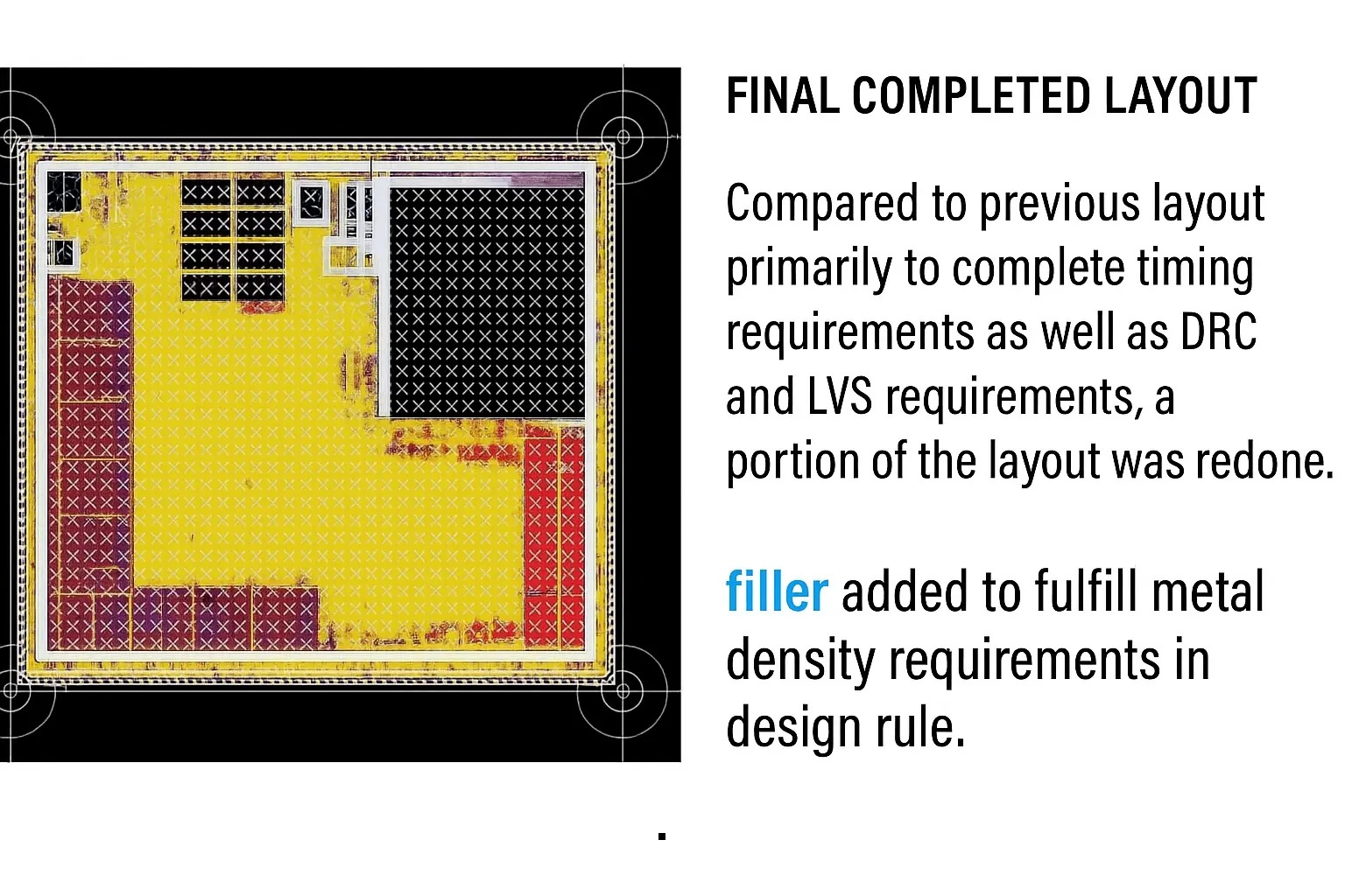
4.6 Layout Physical Verification
Physical verification validates the completed layout across functional and timing aspects and typically includes:
- LVS (Layout vs Schematic): verify the layout matches the synthesized netlist.
- DRC (Design Rule Checking): verify spacing, widths, and other process rules.
- ERC (Electrical Rule Checking): detect shorts, opens, and other electrical violations.
The back-end flow also includes power analysis and design-for-manufacturability (DFM) checks. The final physical layout is delivered to the foundry in GDSII format for wafer fabrication.
After fabrication, packaging and final testing produce the physical chips delivered to customers.