Designing a printed circuit board (PCB) for high-current applications using 1 oz copper can be a challenging yet rewarding task. If you're searching for guidance on "high current 1 oz copper PCB" design, you're in the right place. This blog post offers a comprehensive guide to mastering the techniques and best practices for creating efficient and reliable PCBs that handle significant electrical loads. We'll cover key topics like trace width calculations, thermal management with vias, and essential design rules to ensure your 1 oz copper PCB performs optimally in power distribution and high-current scenarios.
Whether you're an engineer working on power electronics or a hobbyist stepping into advanced designs, this detailed guide will walk you through actionable strategies and proven methods. Let's dive into the world of high-current PCB design with 1 oz copper and explore how to make your projects safe, efficient, and durable.
Understanding 1 oz Copper in High-Current PCB Design
When it comes to PCB manufacturing, copper weight plays a critical role in determining how much current a board can handle. The term "1 oz copper" refers to a copper layer thickness of 1 ounce per square foot, which translates to approximately 1.4 mils or 35 micrometers. This is the standard copper thickness for many PCB designs due to its balance of cost, manufacturability, and performance. However, when designing a "high current 1 oz copper PCB," you must carefully consider its limitations and optimize the layout to prevent issues like overheating or voltage drops.
In high-current applications, such as power supplies or motor controllers, the copper traces need to carry significant electrical loads without failing. A 1 oz copper layer can handle moderate current levels, but pushing it to its limits requires precise design techniques. Understanding the current-carrying capacity of 1 oz copper—typically around 1-2 amps per 10 mils of trace width under standard conditions—is the starting point for any successful design.
Key Challenges in High-Current Design with 1 oz Copper
Designing a PCB for high current with 1 oz copper presents several challenges. The primary concern is heat dissipation, as excessive current can cause traces to overheat, leading to potential board failure or reduced lifespan. Additionally, voltage drops across long or narrow traces can affect performance, especially in power distribution systems. Signal integrity may also be impacted if high-current traces are placed too close to sensitive signal lines.
Another challenge is ensuring that the PCB can withstand the mechanical stress caused by thermal expansion during operation. With 1 oz copper, the thinner layer is more susceptible to damage compared to heavier copper weights like 2 oz or more. Overcoming these challenges requires a combination of strategic layout planning, accurate calculations, and adherence to design rules tailored for "1 oz copper PCB power distribution."
Calculating Trace Width for High Current 1 oz Copper
One of the most critical aspects of high-current PCB design is determining the appropriate trace width to safely carry the required current. For a "trace width for high current 1 oz copper," the width must be calculated based on the expected current load and the acceptable temperature rise. A common guideline is to use a trace width calculator or refer to standards like IPC-2221, which provides charts for current-carrying capacity based on copper thickness and temperature rise.
For example, a 1 oz copper trace with a width of 50 mils (0.05 inches) can typically handle around 2.5 amps with a temperature rise of 10°C above ambient. If your application requires 5 amps, you would need to double the width to approximately 100 mils to keep the temperature rise within safe limits. Keep in mind that external factors, such as ambient temperature and the presence of nearby heat sources, can affect these values.
It's also wise to add a safety margin of at least 20-30% to your calculations to account for unexpected current spikes or manufacturing variations. Using wider traces or splitting the current across multiple parallel traces can further enhance reliability in high-current designs.
Thermal Management with Thermal Vias in 1 oz Copper PCB
Heat is the enemy of high-current PCB designs, and effective thermal management is essential for maintaining performance and longevity. When working with a "thermal vias 1 oz copper PCB," thermal vias act as conduits to transfer heat from the top copper layer to inner layers or a heat sink on the opposite side of the board. These vias are small holes filled or plated with copper that improve thermal conductivity across the PCB stack-up.
For instance, placing an array of thermal vias under high-current components like power transistors or voltage regulators can significantly reduce localized heating. A typical design might use vias with a diameter of 0.3 mm spaced 1 mm apart in a grid pattern to maximize heat dissipation. However, avoid placing too many vias, as this can weaken the board's structural integrity or interfere with routing.
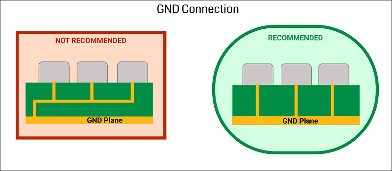
In addition to thermal vias, consider using larger copper pours or planes for heat spreading. A solid ground plane on an inner layer connected via thermal vias can act as a heat sink, distributing thermal energy more evenly across the board. Combining these techniques ensures that your 1 oz copper PCB remains within safe operating temperatures even under high-current loads.
1 oz Copper PCB Design Rules for High-Current Applications
Following specific "1 oz copper PCB design rules" is crucial for creating a board that can handle high current without failure. These rules encompass various aspects of the design process, from trace layout to component placement. Below are some essential guidelines to keep in mind:
- Minimize Trace Length: Keep high-current traces as short as possible to reduce resistance and voltage drops. For example, a 1-inch trace with 1 oz copper at 5 amps might cause a voltage drop of 0.05V, which could be significant in low-voltage systems.
- Use Copper Pours: Implement large copper areas or planes for power and ground connections to distribute current evenly and reduce heat buildup.
- Avoid Sharp Corners: Design traces with smooth, rounded corners instead of sharp 90-degree bends to prevent current crowding and potential hotspots.
- Separate High-Current and Signal Traces: Place high-current traces away from sensitive signal lines to avoid electromagnetic interference (EMI). A spacing of at least 3 times the trace width is a good starting point.
- Consider Layer Stack-Up: In multilayer boards, dedicate entire layers to power and ground planes to enhance current distribution and provide shielding for signal layers.
Adhering to these design rules ensures that your PCB can handle high current while maintaining reliability and performance. Always simulate or prototype your design to validate these parameters under real-world conditions.
Optimizing Power Distribution in 1 oz Copper PCBs
Efficient "1 oz copper PCB power distribution" is at the heart of high-current design. Poor power distribution can lead to uneven current flow, voltage drops, and overheating, all of which compromise the system's performance. To optimize power distribution, start by designing a robust power delivery network (PDN) that minimizes impedance between the power source and the load.
One effective strategy is to use a star topology for power distribution, where each high-current component connects directly to the power source through dedicated traces or planes. This approach reduces the risk of voltage drops caused by shared current paths. Additionally, place decoupling capacitors close to power pins of active components to filter out noise and stabilize voltage levels. A typical value might be a 0.1 μF ceramic capacitor paired with a larger 10 μF capacitor for bulk storage.
Another tip is to balance the current load across multiple traces or layers. For example, if a single trace cannot handle the required current, split the load across two or more parallel traces of equal width and length. This not only reduces resistance but also improves heat dissipation across the board.
Material and Manufacturing Considerations for High-Current PCBs
While 1 oz copper is the focus of this design, the choice of substrate material and manufacturing processes also impacts the performance of high-current PCBs. Standard FR-4 material is suitable for many applications, but for designs with significant thermal stress, consider high-Tg (glass transition temperature) FR-4 or even metal-core PCBs for better heat dissipation.
During manufacturing, ensure that the PCB fabricator can achieve the required trace widths and spacing for your high-current design. Tighter tolerances might be necessary to maintain the integrity of narrow traces carrying high current. Also, verify that the board finish, such as HASL (Hot Air Solder Leveling) or ENIG (Electroless Nickel Immersion Gold), supports high-current connections without degrading over time.
Simulation and Testing for High-Current 1 oz Copper PCBs
Before finalizing your design, use simulation tools to analyze current flow, thermal performance, and voltage distribution. Software packages often include features for thermal analysis and current density mapping, helping you identify potential hotspots or weak points in your layout. For example, a simulation might reveal that a 50-mil trace reaches a temperature of 60°C at 3 amps, prompting you to widen the trace or add thermal vias.
After fabrication, thoroughly test the PCB under load conditions that mimic real-world usage. Use a thermal camera to check for unexpected heat buildup and measure voltage drops across critical traces. Iterative testing and refinement are key to ensuring that your high-current 1 oz copper PCB meets performance expectations.
Conclusion: Mastering High-Current Design with 1 oz Copper
Designing a high-current PCB with 1 oz copper requires careful planning, precise calculations, and adherence to best practices. By focusing on trace width optimization, thermal management with vias, and robust power distribution strategies, you can create a reliable and efficient board for demanding applications. Remember to follow essential "1 oz copper PCB design rules" and leverage simulation tools to validate your design before manufacturing.
With the techniques outlined in this guide, you're well-equipped to tackle the challenges of "high current 1 oz copper PCB" design. Whether you're working on power electronics, automotive systems, or industrial controls, these best practices will help you achieve a balance of performance, cost, and reliability. Start applying these strategies in your next project and take your PCB designs to the next level.
 ALLPCB


