 ALLPCB


Overview
When an amplifier experiences an external overvoltage, ESD diodes are the last line of defense between the amplifier and the overstress. Correctly understanding how ESD cells are implemented inside a device allows designers to extend the amplifier's survivability through appropriate circuit design. This article introduces common ESD implementation schemes, discusses the characteristics of each approach, and provides guidance on using these cells to improve design robustness.
Introduction
Many applications have inputs that are exposed to the external world rather than being fully controlled by the system, such as test equipment, instruments, and some sensing devices. For these applications, input voltages may exceed the front-end amplifier's rated maximum. Protection schemes are therefore required to preserve the design's operating range and robustness. Internal ESD diodes of front-end amplifiers are sometimes used to clamp overvoltage events, but several factors must be considered to ensure this clamping provides reliable protection. Understanding different internal ESD diode architectures and the thermal and electromigration effects of specific protection circuits helps designers address protection-related issues and improve field life.
ESD Diode Configurations
Not all ESD diodes are simple clamps tied to supply and ground. Many configurations are possible, including diode stacks, diode plus resistor, and back-to-back diodes. The following sections describe several common schemes.
Diode to Supply
Figure 1 shows an example amplifier with diodes connected between the input pin and the supply. Under normal operation the diodes are reverse biased, but they become forward biased when the input exceeds the positive supply or goes below the negative supply. When the diodes conduct, current flows from the input pin to the corresponding supply.
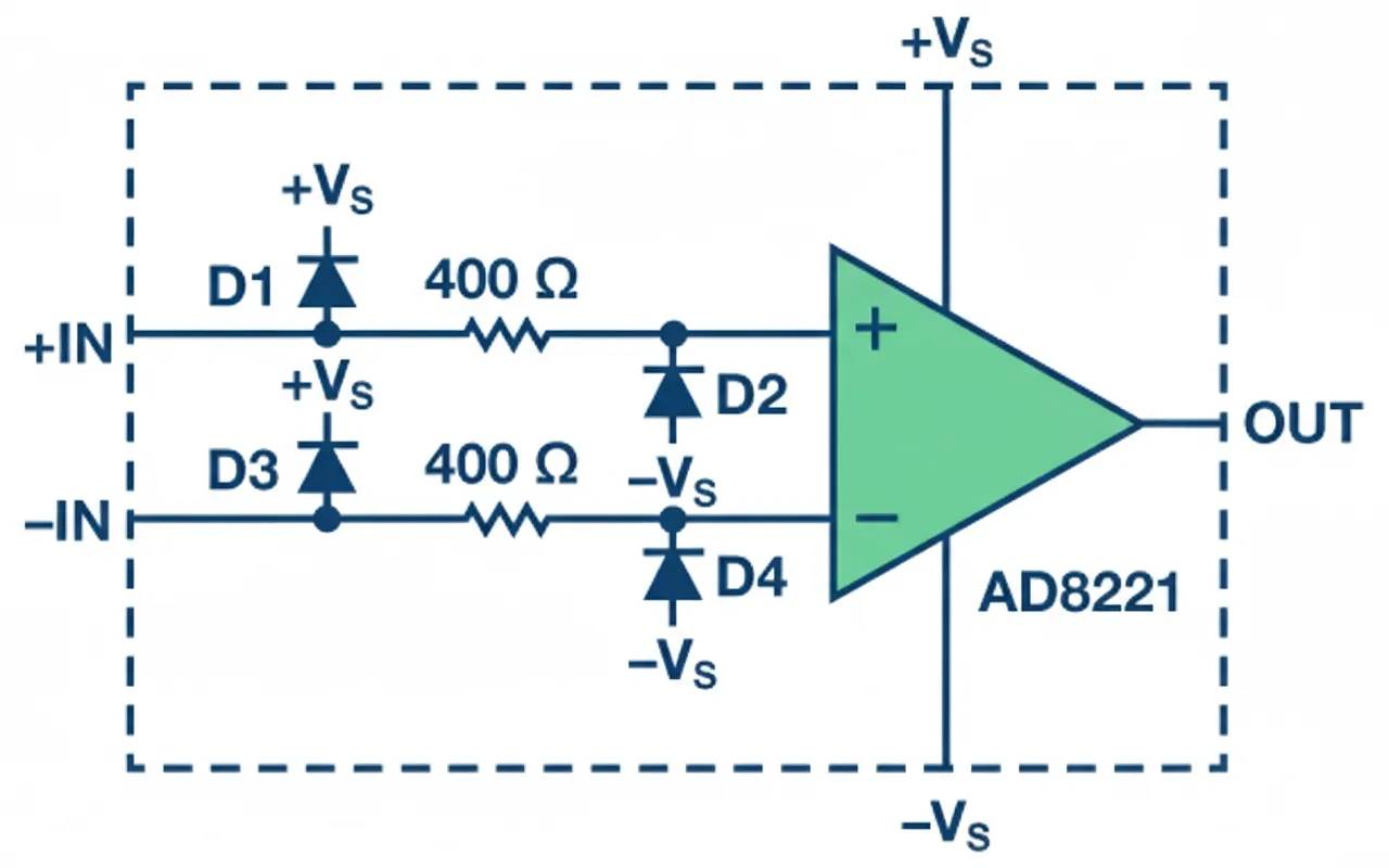
Figure 1. AD8221 input ESD topology
For the circuit in Figure 1, the amplifier itself does not limit input current when the overvoltage exceeds +Vs; an external series resistor is required to limit current. When the voltage is below ?Vs, the 400 Ω resistor provides some current limiting and should be considered in the design.
Figure 2 shows a similar diode-to-supply configuration, but in this case the current is limited by an internal 2.2 kΩ series resistor. The difference from Figure 1 is not only the value of the series resistor R, but also that the 2.2 kΩ resistor can protect the circuit from voltages above +Vs. This example highlights that designers must fully understand the internal protection to optimize their external protection.
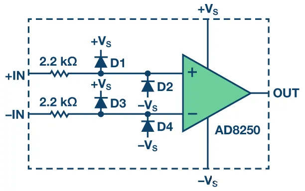
Figure 2. AD8250 input ESD topology
Current-Limiting JFET
Rather than diode clamping, some IC designs use a current-limiting JFET. Figure 3 shows an example where the JFET protects the device when the input voltage exceeds the rated operating range. The JFET input allows the device to tolerate up to 40 V on the opposite supply rail. Because the JFET limits current into the input pin, the ESD cell cannot be used as additional overvoltage protection.
When up to 40 V protection is required, the JFET provides a strictly controlled, reliable protection scheme. This contrasts with diode-based protection, where diode current-limiting information is often specified as typical values or may be unclear.
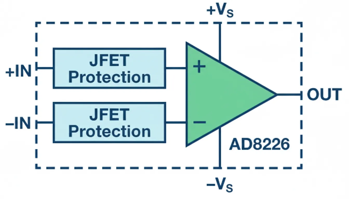
Figure 3. AD8226 input protection scheme
Diode Stacking
In applications that allow the input voltage to exceed the supplies, diode stacks can prevent input damage during ESD events. The amplifier shown in Figure 4 uses stacked diodes. The string is used to limit leakage current within the allowed input range but provides protection when the negative common-mode range is exceeded. Remember that the diode string's equivalent series resistance provides current limiting. For a given voltage, an external series resistor can reduce input current further.
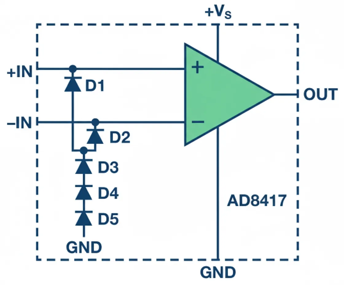
Figure 4. AD8417 low-end input protection
Back-to-Back Diodes
Back-to-back diodes are another option when the allowable input range exceeds the supplies. The amplifier in Figure 5 uses back-to-back diodes for ESD protection and, with a 3.3 V supply, allows voltages up to 70 V. D4 and D5 are high-voltage diodes intended to withstand high voltages on the input pin; D1 and D2 prevent leakage within the normal operating range. In this configuration, using these ESD cells as overvoltage protection is not recommended, because exceeding the maximum reverse voltage of the high-voltage diodes can easily damage the device.
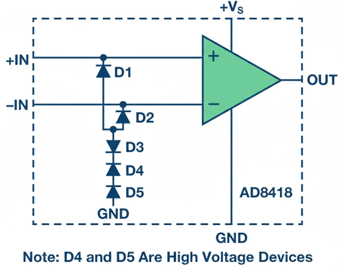
Figure 5. AD8418 high-end input protection
No ESD Clamp
Some devices do not include ESD components at their front end. Clearly, without ESD diodes a designer cannot rely on them for clamping. This architecture is worth noting when evaluating overvoltage protection. The device in Figure 6 uses only a high-value resistor to protect the amplifier.
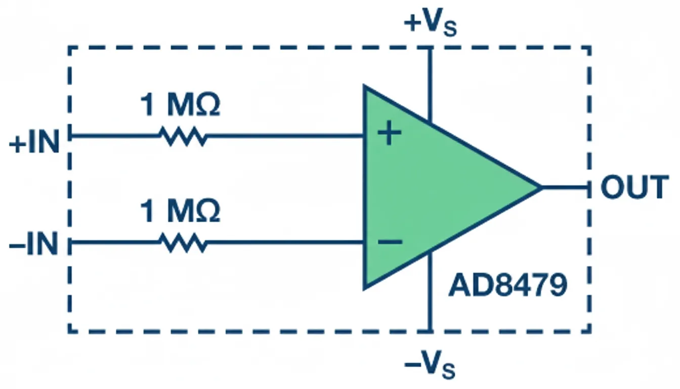
Figure 6. AD8479 input protection
Using ESD Units for Clamping
Beyond understanding how ESD units are implemented, designers must know how to use these structures for protection. Typical practice employs series resistance to limit current during ratings-conforming overvoltage conditions.
When the amplifier is configured as shown in Figure 7, or when the input is protected by diodes tied to the supply, the input current limit can be calculated using the following relation.

Figure 7. ESD unit used for clamping
The formula assumes VSTRESS > VSUPPLY. If that is not the case, measure a more accurate diode voltage and use it for the calculation rather than assuming 0.7 V.
Example calculation: an amplifier powered from ±15 V must withstand input overvoltage up to ±120 V, while limiting input current to 1 mA. Using the formula above, the calculation yields:
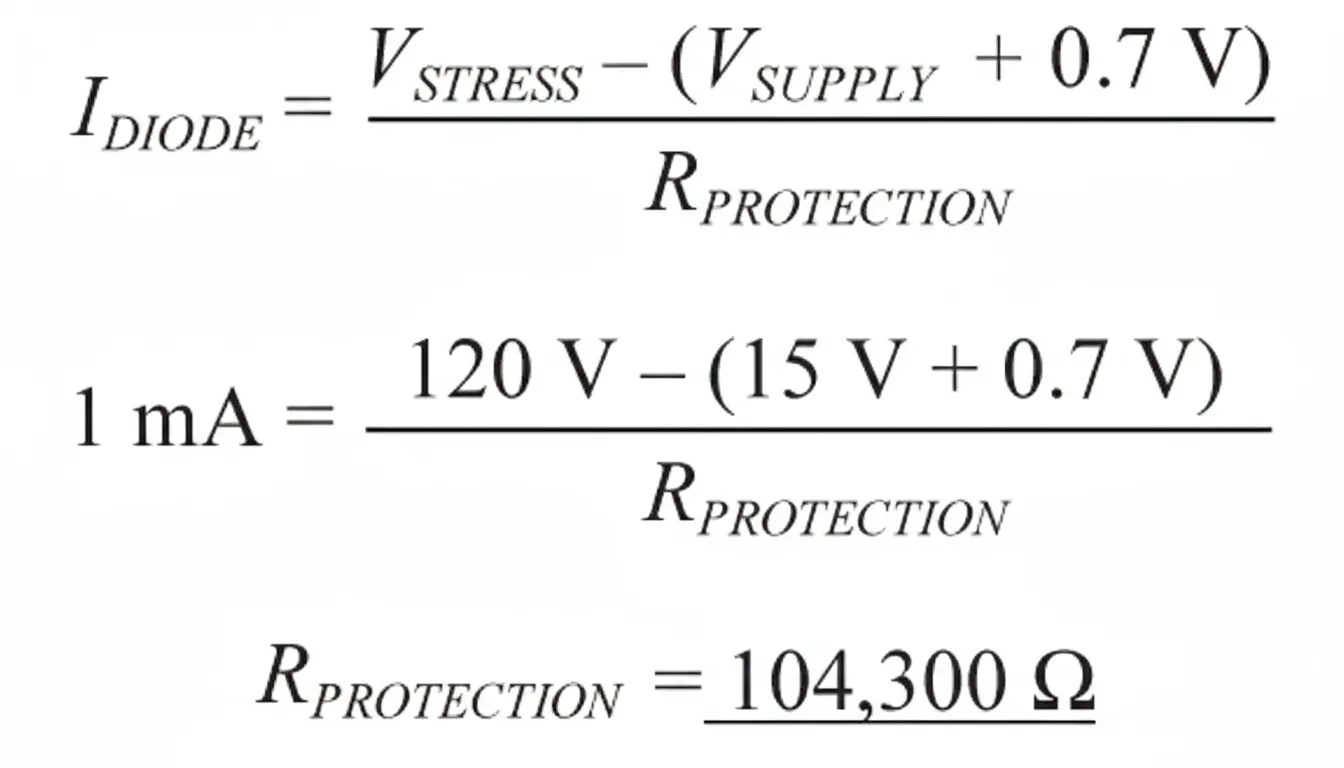
With the stated requirements, RPROTECT > 105 kΩ will limit diode current to below 1 mA.
Understanding Current Limiting
The maximum IDIODE varies by device and depends on the specific application scenario of the applied overvoltage. A single, millisecond-duration event has a different allowable current than a continuous current applied over the device's 20+ year life. Guidance values are available in amplifier datasheets under absolute maximum ratings or in application notes, and are typically in the 1 mA to 10 mA range.
Failure Modes
The maximum current rating of a protection scheme is ultimately limited by two factors: thermal effects from diode power dissipation and the maximum current rating of the current path relative to electromigration. Power dissipation should remain below thresholds that cause excessive junction temperature; the chosen current must stay within ratings to avoid electromigration-related reliability issues.
Thermal Effects
When current flows through an ESD diode, the diode's power dissipation raises temperature. Most amplifier datasheets specify thermal resistance (typically theta_JA), which relates junction temperature rise to power. Considering worst-case ambient temperature and the worst-case temperature rise due to dissipation indicates whether the protection circuit is adequate.
Electromigration
Even if current does not create thermal issues, diode current can still cause reliability problems via electromigration. Every electrical current path has a maximum long-term allowable current due to electromigration. The electromigration limit for the diode current path is often constrained by the thickness of internal metal traces in series with the diode. Manufacturers may not publish this information, so long-term continuous diode currents require careful consideration.
For example, electromigration can be a concern when an amplifier monitors a voltage rail that is independent of its own supplies. Multiple power domains can lead to temporary voltages that exceed absolute maximum conditions due to power sequencing. Considering worst-case current paths and the duration of those currents over the product lifetime, combined with knowledge of maximum allowable electromigration current, helps avoid reliability issues.
Conclusion
Understanding how internal ESD diodes activate during overstress helps designers improve robustness. Evaluating the thermal impact and electromigration effects of protection circuits highlights potential problems and whether additional protection is necessary. Considering the conditions outlined here enables designers to make informed choices and avoid field robustness failures.


