1. Principles of Electrostatic Generation
All matter is composed of atoms containing positively charged protons and negatively charged electrons. In a neutral state, the positive charge of the protons balances the negative charge of the electrons. However, processes like friction, contact, or separation can cause electrons to move between objects. An object that gains excess electrons becomes negatively charged, while an object that loses electrons becomes positively charged. This phenomenon, known as static electricity, can occur on all types of materials, including conductors and semiconductors.
2. Types of Charging
Contact Charging: Static electricity is commonly generated when two objects come into contact and are then separated. This is one of the most frequent forms of static generation.
Frictional Charging (Triboelectric Effect): Rubbing two objects together generates heat and causes a transfer of electrons, resulting in static charge. The amount of charge generated depends on factors such as the degree of contact, surface uniformity, contact pressure, friction force, and separation speed.
Induction Charging: This occurs when an uncharged object is placed within the electric field of a charged object. For example, a component can become charged when brought near a statically charged plastic bag, even without direct contact.
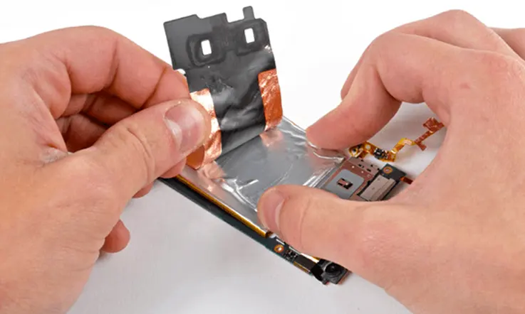
Separation Charging: Static electricity is generated when adhered materials are peeled apart, such as removing adhesive tape or labels. It also occurs when a belt separates from a pulley in a rolling system.
Spray Charging: When liquids or gases are ejected through a nozzle, friction between the sprayed particles and the nozzle can generate static electricity. Air guns and cooling fans are common examples of devices that can cause spray charging.
Thermionic Emission: When a material is heated, electrons in its outermost orbital gain energy, making them more likely to escape from the atom. In a vacuum or low-pressure gas, this emission of electrons can lead to charging.
Photoelectric Charging: When light, particularly ultraviolet (UV) radiation, strikes a material's surface, it can dislodge electrons, leaving a positive charge on the surface. Prolonged exposure of electronic products to sunlight can generate static electricity through this effect.
3. Triboelectric Series
The triboelectric series is a list that ranks materials according to their tendency to gain or lose electrons. Materials at the top of the series have a strong tendency to become positively charged, while materials at the bottom have a strong tendency to become negatively charged.
4. ESD-Induced Failures
Any PCB can be affected by an electrostatic discharge event if it comes into contact with or is brought near a person, packaging, cable, or any other object with a significant potential difference. If this voltage difference is large enough, a current path will form, creating a strong current pulse. This pulse can generate intense heat in component leads and PCB traces. In cases of extreme electric field strength and discharge current, PCB traces can be damaged and components can be destroyed.
5. ESD Sensitivity of Common Devices
| Device Type | ESD Voltage Range (V) |
|---|---|
| VMOS | 30-1800V |
| MOSFET | 100-200V |
| GaAs FET | 100-300V |
| EPROM | 100V |
| JFET | 140-7000V |
| SAW | 150-500V |
| OP-AMP | 190-2500V |
| CMOS (Input Protected) | 250-3000V |
| Schottky Diodes | 300-2500V |
| Film Resistors | 300-3000V |
| Bipolar Transistors | 380-7000V |
| ECL (PCB Level) | 500V |
| SCR | 680-1000V |
6. ESD Risks in Production and Storage
Scenario: 2000V ESD
Problem: Component packaging bags generate 2kV of static electricity.
Solution: Replace with anti-static packaging bags.
Scenario: 10,000V ESD
Problem: ICs are placed on static-generating foam.
Solution: Use dedicated anti-static IC trays or jigs.
Scenario: 9,000V ESD
Problem: ICs are placed on static-generating foam.
Solution: Use dedicated anti-static IC trays or jigs.
Scenario: 5,000V ESD
Problem: Components are mixed with standard packaging materials.
Solution: Remove all non-essential, static-generating packaging.
Scenario: 2,000V ESD
Problem: Component storage boxes are made from non-anti-static materials.
Solution: Line the boxes with anti-static mats.
7. PCB-Level ESD Protection
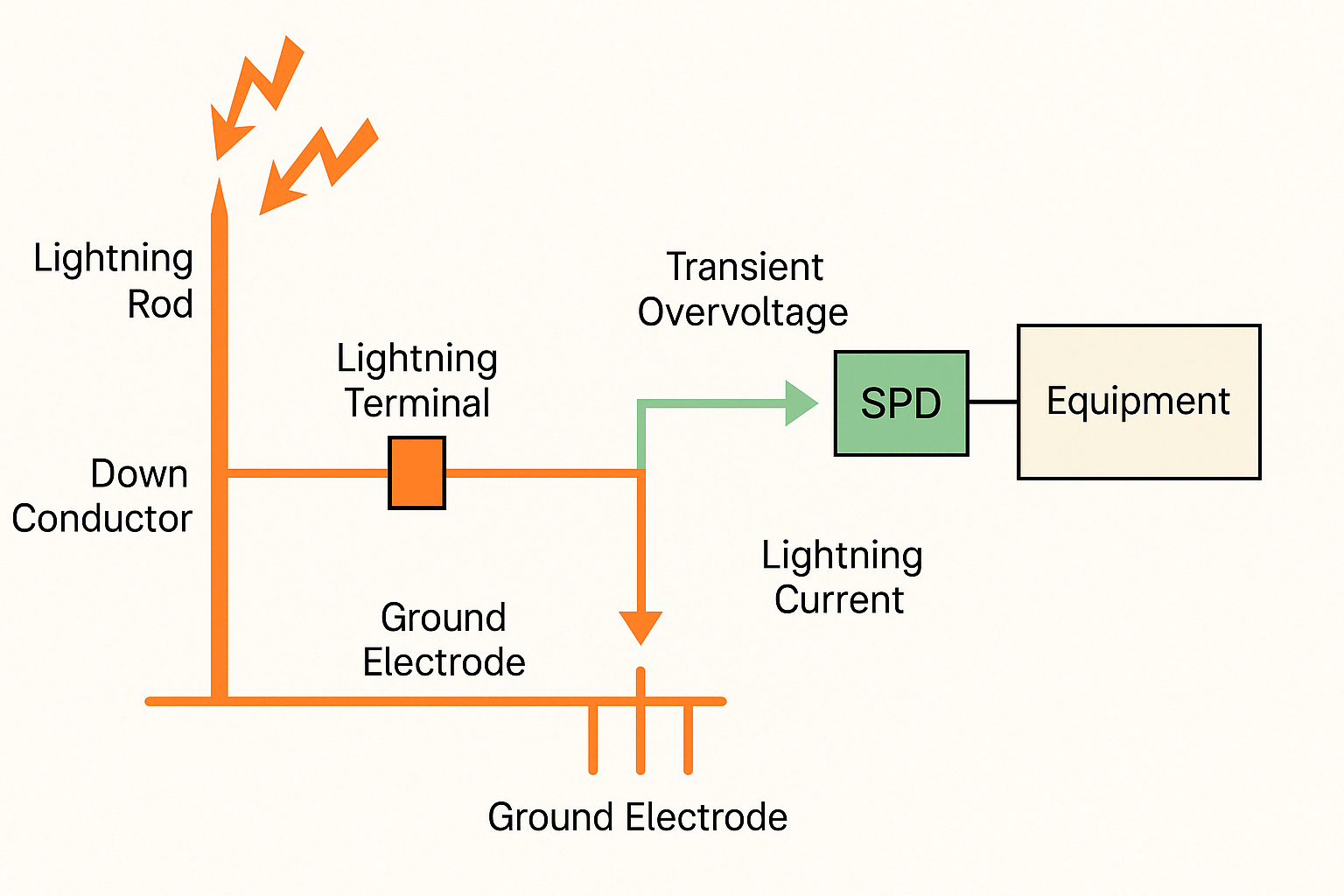
The goal of on-PCB ESD protection is to divert ESD current away from sensitive circuitry and channel it to ground through a low-impedance path. Under normal operating conditions, the protection components should not affect the signals on the lines they protect. An ESD protection circuit should only activate during an ESD event, responding quickly within the pulse's rise time to divert the energy.
Ideally, the ESD pulse should be shunted to the system ground. The preferred grounding options, in order of priority, are:
- Chassis ground connected to earth ground.
- Chassis ground connected to system ground at a point far from the likely ESD entry point.
- A guard ring on the PCB, connected to system ground as in the second case.
- System ground.
The best practice is to keep the discharge path off the PCB entirely, which is why chassis ground is the preferred discharge point for both ESD protection and fault currents.
A common circuit used on the I/O lines of integrated circuits near potential ESD sources (like connectors) employs Zener diodes, often in the form of a transient voltage suppressor (TVS) array. A typical TVS array uses four Zener diodes that are reverse-biased during an ESD event, creating a shunt path for the ESD voltage/current to protect the load components. These devices should be placed as close as possible to the ESD source so that the current can be immediately diverted to ground.
Another option is a standalone TVS diode, which is a common method for implementing ESD protection on critical interfaces. Although called a diode, a TVS device is a more complex component, as shown by its equivalent circuit.
Other ESD protection devices include gas discharge tubes (GDTs) and simple varistors. GDTs are typically used for slower, high-energy events like power surges, rather than fast ESD events. Before using any component for ESD protection, always check its datasheet to understand its response time and specifications.
8. ESD Protection in Manufacturing
Anti-static Mats: These are classified by use (table mats, floor mats) and material (conductive, dissipative, insulative). They provide a surface where static charges can be safely discharged.
Anti-static Garments: Work clothes made from fabrics with interwoven conductive fibers (e.g., carbon or metal) are common and effective. In contrast, synthetic materials like acrylics are prone to generating high levels of static electricity.
Ionizers (Ionizing Air Blowers): Ionizers are effective for neutralizing static charges on insulative materials that cannot be grounded, such as plastics. Different products have different characteristics, so it is important to follow the manufacturer's instructions regarding safe operating distance, cleaning schedules, and calibration cycles.
Anti-static Liquids/Sprays: These are available in two main types:
- Surfactants that apply a conductive layer to a surface, allowing it to be grounded.
- Hygroscopic chemicals that attract moisture from the air to form a conductive or dissipative layer, preventing static buildup.
The effectiveness of these treatments can diminish over time as the surface layer wears off or dries out. Therefore, periodic reapplication and verification are necessary.
9. Human Perception of Static Discharge
| Body Voltage | Sensation | Notes |
|---|---|---|
| 1.0kV | No sensation | A faint discharge sound may occur. |
| 2.0kV | Slight sensation at fingertip, no pain | |
| 2.5kV | Startling, like a pinprick, but not painful | |
| 3.0kV | Slight pain, like a light needle poke | Discharge spark may be visible. |
| 4.0kV | Fingertip feels a slight, sharp pain | Spark visible at fingertip. |
| 5.0kV | Painful shock to the palm or wrist | (Note: Assumes human body capacitance of 90pF) |
| 6.0kV | Painful shock to the finger, arm feels the jolt | |
| 7.0kV | Strong pain and numbness in finger and palm | |
| 8.0KV | Numbness felt in hand and arm | |
| 9.0kV | Strong pain in wrist with numbness | |
| 10.0kV | Entire hand feels pain, like an electric shock | |
| 11.0kV | Strong numbness in fingers, intense shock to hand | |
| 12.0kV | Body feels the jolt from the intense shock |
10. PCB Layout Techniques for ESD Protection
1. Use Ground Planes: Use a solid ground plane covering as much of the PCB as possible and ensure all ground connections are solid. A ground plane provides effective shielding and a low-impedance path for discharge currents.
2. Route Traces Carefully: Route sensitive signal traces as close as possible to their corresponding ground traces or plane, and keep them parallel to minimize loop area and reduce induced noise.
3. Use Differential Signaling: For high-speed and sensitive signals, using differential pairs provides better immunity to ESD and other common-mode noise.
4. Add Filtering: Place filters on signal lines to help suppress ESD pulses and other high-frequency noise.
5. Place Protection Components Strategically: Place ESD protection components like TVS diodes near connectors and other entry points. These components absorb and divert ESD energy, protecting downstream circuitry.
6. Avoid Sharp Corners: Avoid sharp 90-degree corners in traces, as they can create points of high electric field concentration, increasing the risk of dielectric breakdown during an ESD event. Use 45-degree bends or curved traces instead.
7. Isolate Power and Ground: Carefully route power and ground traces to minimize coupling and prevent ESD from propagating through the power distribution network.
8. Ensure Solid Return Paths: Provide direct, low-impedance return paths for ground currents to ensure ESD energy can be effectively shunted away from sensitive circuits.
 ALLPCB


