ALLPCB


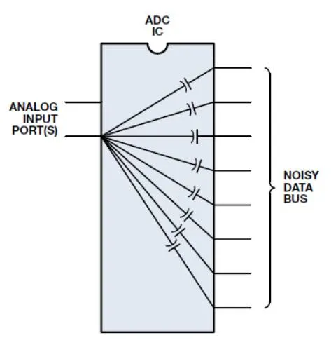
Isolation and buffering of ADC digital outputs
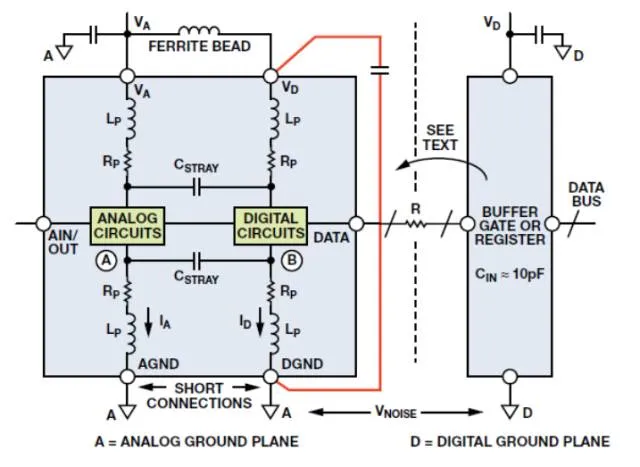
Although many converters provide three-state outputs/inputs, the associated registers still exist on the chip. They allow data pins to couple to sensitive regions, so isolation buffers remain a good design practice. In some cases, additional data buffers placed adjacent to the converter outputs on the analog ground plane are used to improve isolation.
Placing a data buffer next to the converter helps isolate digital outputs from data-bus noise (see Figure 1). Buffers also minimize loading on the converter’s digital outputs and provide a Faraday-type shield between the digital outputs and the data bus (see Figure 2).
Series resistor and RC filtering
The series resistor between an ADC output and a buffer-register input (marked "R" in Figure 1) helps minimize digital transients that can affect converter performance. The resistor isolates the digital output driver from the input capacitance of the buffer register. The series resistor together with the buffer-input capacitance forms an RC network that acts as a low-pass filter to slow fast edges.
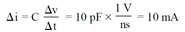
A typical CMOS gate plus PCB traces and vias produce about 10 pF of load. Without a series resistor, a logic output with 1 V/ns slew rate will generate about 10 mA of dynamic current.
Avoid TTL registers because their higher input capacitance significantly increases dynamic switching current.
Grounding and decoupling for digital circuits
Buffer registers and other digital circuits should be grounded and decoupled to the PCB digital ground plane. Note that any noise between analog and digital ground planes reduces noise margin on the converter’s digital interface. Since digital noise immunity is typically in the hundreds to thousands of millivolts, this is usually not problematic. Analog ground plane noise is normally low, but if digital ground noise (relative to the analog ground) exceeds a few hundred millivolts, steps should be taken to reduce digital ground impedance to keep the noise margin acceptable. In no case should the voltage between the two ground planes exceed 300 mV, as IC damage may occur.
Power supplies and decoupling
It is best to provide separate supplies for analog and digital sections. The analog supply should power the converter. If the converter specifies a separate digital supply pin (VD), it should be supplied from a separate analog-derived supply or filtered as shown in Figure 3. All converter supply pins should be decoupled to the analog ground plane, and all logic supply pins should be decoupled to the digital ground plane, as illustrated in Figure 3. If the digital supply is relatively quiet, it may be used to power analog circuits, but exercise caution.
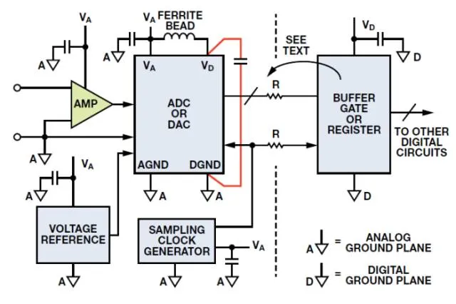
In some cases VD cannot be tied to the analog supply. Some high-speed ICs use +5 V for analog sections and +3.3 V or lower for the digital interface to match external logic. In such cases the IC’s +3.3 V pin should be decoupled directly to the analog ground plane. It is also recommended to place a ferrite bead in series with the power trace to connect the pin to the +3.3 V digital logic supply. The sampling clock generation circuitry should be treated like the analog circuitry: referenced to analog ground and deeply decoupled to the analog ground plane.
Grounding for high-frequency operation
Ideally, supply and signal currents should return via a ground plane, which also provides reference nodes for converters, reference sources, and other subsystems. However, widespread use of a ground plane alone does not guarantee a high-quality AC ground reference.
Consider the simple two-layer PCB example in Figure 4: a DC/AC current source on the top layer with one terminal connected to via 1 and the other connected via a U-shaped trace to via 2. Both vias connect to the ground plane. Ideally the ground loop impedance between the top connector and vias 1 and 2 is zero and the voltage across the current source is zero.
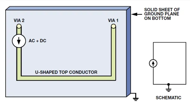
To understand high-frequency grounding issues, examine how current returns in the ground plane from via 1 to via 2.
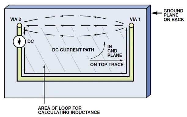
For DC, current chooses the path of least resistance in the ground plane between via 1 and via 2; some spreading occurs but current does not substantially deviate from that path. By contrast, AC current selects the path of least impedance, which depends on inductance.
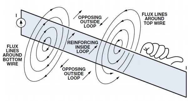
Inductance is proportional to the loop area. Using the right-hand rule and magnetic-field concepts, the magnetic field inside a loop is reinforced by currents flowing around the loop and opposed outside the loop, thus confining the field. Larger loops have higher inductance, store more magnetic energy for a given current, and present higher impedance (XL = jωL), producing greater voltages at a given frequency.
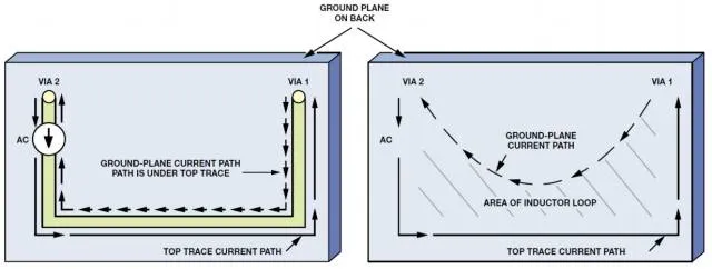
The current will choose the lowest-impedance path in the ground plane. Considering the loop formed by the U-shaped top trace and the ground plane beneath it, and neglecting resistance, high-frequency AC current will flow along the route that minimizes the enclosed area.
In this example the smallest-area loop is formed by the U-shaped top trace and the section of ground plane immediately beneath it. Figure 5 shows the DC path, while Figure 7 shows the AC return path in the ground plane, which sits directly under the U-shaped top trace. In practice, ground-plane resistance causes mid- and low-frequency currents to split between the direct return path and the area under the top trace, but even at frequencies as low as 1 MHz to 2 MHz the return path remains close to the top trace.
Sampling clock considerations
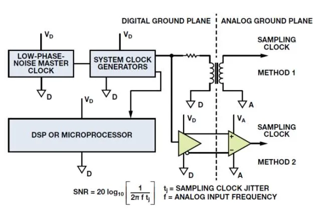
For high-performance sampled-data systems, use a low phase-noise crystal oscillator for the ADC or DAC sampling clock. Sampling-clock jitter modulates the analog I/O and raises the noise and distortion floor. The sampling clock generator should be isolated from noisy digital circuits and referenced and decoupled to the analog ground plane, same as the amplifiers and ADC.
The effect of sampling-clock jitter on ADC SNR can be approximated by:
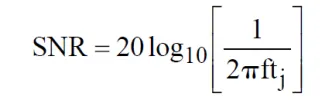
where f is the analog input frequency and SNR is the SNR of an ideal infinite-resolution ADC whose only noise source is rms sampling-clock jitter tj. For example, if tj = 50 ps rms and f = 100 kHz, SNR = 90 dB, about 15 bits of dynamic range.
Note that tj in the example is the root-sum-square of external clock jitter and internal ADC aperture jitter. In most high-performance ADCs, internal aperture jitter is negligible compared to external clock jitter.
Because SNR degradation is primarily due to external clock jitter, the sampling clock must be as noise-free as possible with minimal phase jitter. This requires a crystal oscillator. Several manufacturers provide small crystal oscillators that produce low jitter (under 5 ps rms) with CMOS-compatible outputs.
Ideally the sampling-clock crystal oscillator should reference the analog ground plane in a split-ground system. System constraints may prevent this, so in many cases the sampling clock is derived from a higher-frequency system clock on the digital ground plane and then routed from the digital origin to the ADC on the analog ground plane. Noise between the two ground planes is directly added to the clock and creates excessive jitter, which degrades SNR and generates spurious harmonics.
Transmitting the sampling clock as a differential signal using a small RF transformer (Figure 8) or high-speed differential drivers/receivers can mitigate this problem. If using differential drivers/receivers, choose logic families that minimize phase jitter; ECL is often preferred. In a single +5 V system, ECL can be referenced between ground and +5 V (PECL), with the outputs AC-coupled to the ADC sampling-clock input. In all cases, the system master clock must originate from a low phase-noise crystal oscillator.