 ALLPCB


Separating printed circuit boards (PCBs) from panels without causing damage is a critical step in electronics manufacturing. Whether you're a hobbyist or a professional engineer, using the right PCB depaneling techniques ensures the integrity of your boards and prevents costly defects. In this comprehensive guide, we'll explore effective depaneling methods like V-scoring separation, tab routing breakout, and stress-free depaneling approaches to help you achieve clean and safe separation.
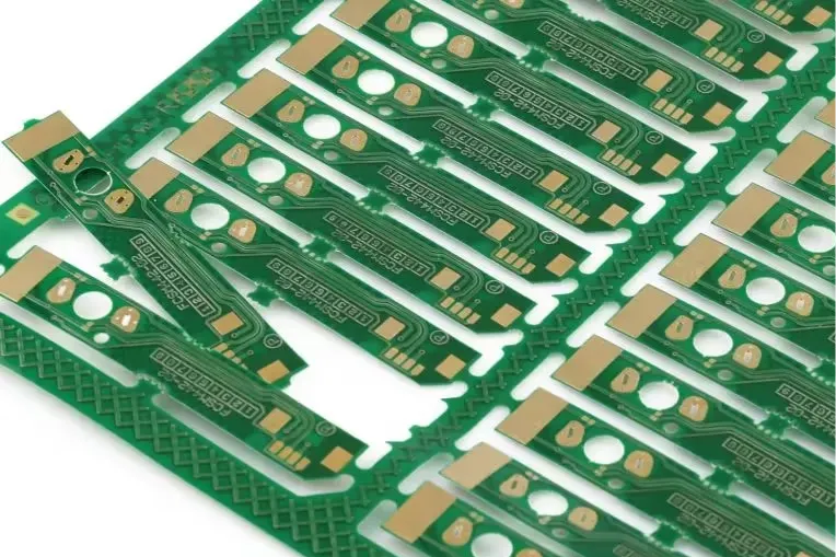
At its core, PCB depaneling is the process of separating individual circuit boards from a larger panel after manufacturing. Panels are used to streamline production, but improper separation can lead to cracks, component damage, or structural weaknesses. By choosing the right method—whether it’s V-scoring for straight cuts or tab routing for complex shapes—you can minimize stress and maintain board quality. Let’s dive into the details of these techniques and how to apply them for optimal results.
What Is PCB Depaneling and Why Does It Matter?
PCB depaneling is the process of separating individual PCBs from a larger panel or array used during manufacturing. Panels allow multiple boards to be fabricated and assembled simultaneously, saving time and reducing costs in high-volume production. However, separating these boards without causing damage is essential to ensure functionality and reliability.
Damage during depaneling can result in microcracks, broken components, or compromised solder joints, especially for delicate surface-mount devices (SMDs). According to industry studies, improper depaneling can lead to failure rates as high as 5-10% in sensitive applications. That’s why selecting the appropriate depaneling method is critical for maintaining board integrity and meeting quality standards.
Key Factors to Consider Before Choosing a Depaneling Method
Before diving into specific techniques, it’s important to understand the factors that influence the choice of depaneling method. These include:
- Board Design and Shape: Simple rectangular boards may work well with V-scoring, while irregular shapes often require tab routing.
- Component Sensitivity: Boards with fragile SMD components need stress-free depaneling to avoid damage.
- Production Volume: High-volume runs may benefit from automated methods, while low-volume or prototype work might use manual techniques.
- Material Thickness: Thicker boards (e.g., above 2.0 mm) may require more robust separation methods to prevent cracking.
- Edge Quality Requirements: Some applications demand smooth edges, which may rule out certain methods like manual breaking.
By evaluating these factors, you can narrow down the most suitable depaneling method for your project and avoid potential issues during separation.
Popular PCB Depaneling Methods for Damage-Free Separation
Let’s explore the most widely used depaneling techniques, focusing on their processes, benefits, and ideal applications. These methods include V-scoring separation, tab routing breakout, and other stress-free depaneling approaches.
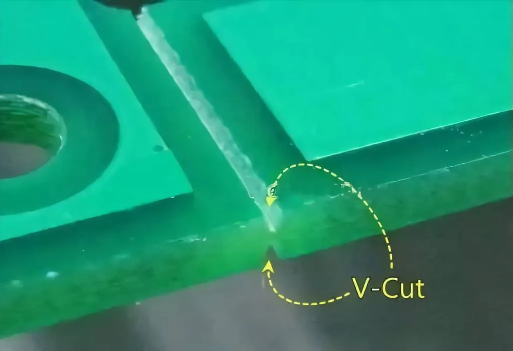
1. V-Scoring Separation: Precision for Straight Cuts
V-scoring is one of the most common PCB depaneling techniques, especially for boards with straight edges. This method involves cutting a V-shaped groove on both sides of the PCB panel using a specialized scoring tool. The groove typically penetrates about one-third of the board thickness from each side, leaving a thin strip of material in the middle that can be easily snapped apart.
How It Works: After the grooves are cut during the manufacturing process, the boards can be separated manually by applying gentle pressure along the scored line or using a fixture for more controlled breaking. For larger volumes, automated V-scoring machines ensure consistent results.
Benefits of V-Scoring Separation:
- Cost-effective for high-volume production.
- Fast and efficient, with minimal setup time.
- Produces relatively clean edges with low stress on components if done correctly.
Limitations:
- Only suitable for straight cuts; not ideal for curved or irregular shapes.
- Can cause stress or microcracks if the board is too thick (e.g., over 2.5 mm) or if snapping isn’t controlled.
- Not recommended for boards with components close to the scored edge (within 0.5 mm), as vibration during breaking can damage them.
Best Use Case: V-scoring is ideal for rectangular boards in high-volume production where straight separation lines are needed, and components are placed away from the edges.
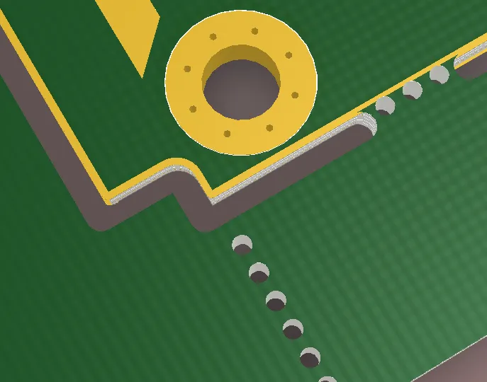
2. Tab Routing Breakout: Flexibility for Complex Shapes
Tab routing, also known as breakaway tab depaneling, is a versatile method that works well for PCBs with irregular shapes or when V-scoring isn’t feasible. This technique involves routing most of the material between individual boards while leaving small, strategically placed tabs (or bridges) to hold the panel together during manufacturing.
How It Works: Small holes, often called "mouse bites," are drilled into the tabs to weaken them. After assembly, the tabs can be broken manually or with a tool to separate the boards. Alternatively, edge rails (breakaway rails) can be added to the panel’s perimeter for extra protection during handling, which are also removed during depaneling.
Benefits of Tab Routing Breakout:
- Supports complex board shapes and curved edges.
- Reduces stress compared to V-scoring since there’s no snapping involved in critical areas.
- Edge rails protect board edges during manufacturing and assembly.
Limitations:
- Leaves rough edges or small tab remnants, which may require additional finishing for aesthetic or functional reasons.
- More time-consuming to design and fabricate compared to V-scoring due to precise routing and tab placement.
- Manual breaking of tabs can introduce minor stress if not done carefully.
Best Use Case: Tab routing is perfect for non-rectangular boards or designs where components are near the edges, and flexibility in separation lines is needed.
3. Stress-Free Depaneling: Protecting Sensitive Components
For boards with delicate components or high reliability requirements, stress-free depaneling methods are essential. These techniques prioritize minimizing mechanical stress and vibration during separation to protect solder joints and SMD components.
Common Stress-Free Depaneling Methods:
- Laser Cutting: Uses a focused laser beam to cut through the PCB material with precision. It produces clean edges and no mechanical stress, making it ideal for thin boards (under 1.6 mm) or those with components near the cut line. However, it’s more expensive and slower for high-volume production.
- Pizza Cutter (Rotary Blade): A manual or motorized rotary blade cuts along pre-scored lines, offering a low-stress alternative to snapping. It’s often used with V-scored panels for controlled separation.
- Automated Routers: High-precision CNC routers cut through panels without manual intervention, reducing the risk of human error and ensuring consistent, stress-free separation. They’re suitable for both tab routing and custom shapes.
Benefits of Stress-Free Depaneling:
- Minimizes risk of damage to sensitive components like SMDs or BGAs.
- Produces high-quality edges with little to no cleanup needed (especially with laser cutting).
- Ideal for prototypes or high-value boards where reliability is critical.
Limitations:
- Higher costs, especially for laser cutting or automated routers.
- Slower processing times compared to manual V-scoring or tab breakout.
- May require specialized equipment or expertise.
Best Use Case: Stress-free depaneling is best for boards with fragile components, thin materials, or applications where edge quality and reliability are non-negotiable, such as in medical or aerospace electronics.
Best Practices for Damage-Free PCB Depaneling
Regardless of the method you choose, following best practices can significantly reduce the risk of damage during depaneling. Here are some actionable tips:
- Design with Depaneling in Mind: Place components at least 0.5-1.0 mm away from separation lines to avoid stress or vibration damage. For V-scoring, ensure straight lines are used in the design phase.
- Use Proper Fixtures: When manually separating boards, use fixtures or jigs to apply even pressure and prevent twisting or bending.
- Test on Prototypes: Before full-scale production, test your chosen depaneling method on a small batch to identify potential issues like cracking or rough edges.
- Optimize Tab Placement: For tab routing, place tabs in areas that minimize stress on critical components, and use mouse bites with 0.2-0.3 mm holes for easier breaking.
- Consider Board Thickness: For thicker boards (above 2.0 mm), avoid manual snapping and opt for automated routers or laser cutting to prevent structural damage.
Implementing these practices can save time, reduce waste, and ensure your PCBs remain intact and functional after separation.
Comparing Depaneling Methods: Which One Suits Your Needs?
To help you decide on the best depaneling method, here’s a quick comparison based on key criteria:
| Method | Best for Shapes | Stress Level | Cost | Speed | Edge Quality |
|---|---|---|---|---|---|
| V-Scoring Separation | Straight Lines | Moderate | Low | High | Moderate |
| Tab Routing Breakout | Complex Shapes | Low to Moderate | Moderate | Moderate | Rough |
| Stress-Free (Laser/Router) | Any Shape | Very Low | High | Low to Moderate | Excellent |
This table highlights the trade-offs between cost, speed, and quality. For instance, if budget is a concern and you’re working with simple designs, V-scoring offers a practical solution. On the other hand, if your priority is protecting sensitive components, investing in stress-free depaneling methods like laser cutting is worth the cost.
Conclusion: Mastering PCB Depaneling for Quality Results
Effective PCB depaneling is a vital part of the manufacturing process that directly impacts the quality and reliability of your circuit boards. By understanding and applying techniques like V-scoring separation, tab routing breakout, and stress-free depaneling, you can separate PCBs from panels without damage and ensure optimal performance in your final product.
Start by assessing your board design, component placement, and production needs to select the right method. Incorporate best practices like proper fixture use and design optimization to further minimize risks. Whether you’re handling high-volume production or delicate prototypes, the right depaneling approach can save time, reduce costs, and maintain the integrity of your PCBs.
With these insights, you’re well-equipped to tackle PCB depaneling challenges and achieve clean, damage-free separation every time. Explore these methods in your next project to see the difference in quality and efficiency.


