ALLPCB


Overview
EDA, electronic design automation, refers to the automated tools and processes used for circuit and chip design. The EDA design flow is typically iterative and consists of the following major stages.
Main steps in the EDA design flow
- Design planning: Define design requirements, objectives, and constraints, including functional specifications, performance targets, and power limits.
- Circuit design: Create schematic-level designs, choose appropriate circuit topologies, and specify functional and performance characteristics.
- Circuit simulation: Use simulation tools to model and verify the design, assessing performance, stability, and correctness.
- Physical layout: Convert the circuit design into a physical layout, placing components and routing interconnects on the chip or board.
- Physical verification: Perform DRC (design rule check) and LVS (layout versus schematic) to ensure the layout complies with manufacturing rules and matches the schematic.
- Timing analysis and optimization: Analyze timing to verify that timing constraints are met and perform optimizations to ensure timing closure.
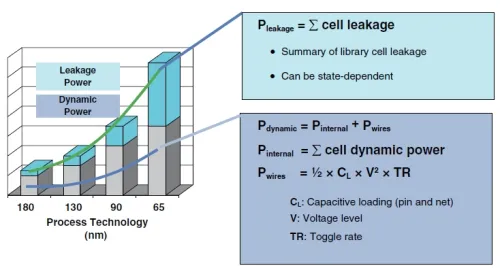
- Power analysis and optimization: Evaluate power consumption and apply techniques to meet power targets.
- Integration and verification: Integrate modules and run functional and system-level verification to ensure correctness and consistency across the design.
- Physical manufacturing preparation: Finalize and repair the layout as needed and generate the masks and process data required for fabrication.
Common EDA software
Tool selection depends on project requirements and workflow. Common tools include:
- Circuit simulation: Cadence Spectre, Synopsys HSPICE, Keysight ADS, Ansys HFSS.
- Logic design and synthesis: Cadence Encounter, Synopsys Design Compiler, Mentor Graphics ModelSim.
- Physical implementation: Cadence Innovus, Synopsys ICC.
- Physical verification: Cadence Virtuoso, Synopsys IC Validator, Mentor Graphics Calibre (for DRC and LVS).
- Timing analysis: Cadence Tempus, Synopsys PrimeTime, Mentor Graphics HyperLynx.
- Power analysis: Cadence Voltus, Synopsys PrimePower, Mentor Graphics Olympus PowerPro.
- FPGA development: Xilinx Vivado, Intel Quartus Prime.
- PCB design: Cadence Allegro, Mentor Graphics PADS, Altium Designer.
Programming and description languages used in EDA
Common languages and scripting tools in EDA include:
- Verilog: a hardware description language used for digital design and simulation across gate, RTL, and behavioral levels.
- VHDL: another HDL for describing and verifying digital systems, comparable to Verilog.
- SystemVerilog: an extension of Verilog that adds verification and advanced design features, including object-oriented constructs and constrained-random verification.
- Tcl: a scripting language widely used to automate and control EDA tools and flows.
Other commonly used languages and tools include MATLAB and Python for algorithm development and data analysis, C/C++ and SystemC for high-level modeling and high-level synthesis, and Perl or shell scripts for automation and flow control. The choice of language depends on tool support, project needs, and team expertise.