 ALLPCB


In the world of PCB manufacturing, applying a dry film solder mask is a critical step to protect circuits and ensure reliable performance. But how is this protective layer applied, and what lamination techniques are used to achieve precision? At ALLPCB, we’re diving into the details of dry film solder mask application, focusing on popular lamination techniques like vacuum lamination and hot roll lamination. Whether you’re an engineer or a hobbyist, this guide will walk you through the process, benefits, and best practices for achieving top-notch results in PCB production.
In this blog, we’ll explore what dry film solder mask is, why it’s essential, and how different lamination methods impact the quality of your printed circuit boards. Let’s get started with a deep dive into the fundamentals and advanced techniques used in the industry.
What Is Dry Film Solder Mask and Why Is It Important?
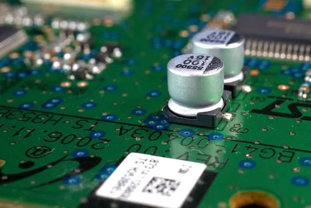
Dry film solder mask is a thin, photosensitive polymer layer applied to the surface of a printed circuit board (PCB). Unlike liquid solder masks, this material comes in a solid film form, sandwiched between two protective layers to shield the photosensitive emulsion during handling. Once applied, it acts as a barrier, protecting copper traces from oxidation, preventing solder bridges during assembly, and insulating conductive elements to avoid short circuits.
The importance of a solder mask in PCB manufacturing cannot be overstated. It enhances the durability of the board by safeguarding it against environmental factors like moisture and dust. Additionally, it ensures precise soldering by defining exact areas where solder should adhere, which is crucial for high-density designs where pads are closely spaced. For example, in boards with impedance control requirements, a uniform solder mask thickness (typically around 0.8 to 1.2 mils) is vital to maintain signal integrity at high frequencies, such as 5 GHz or above in RF applications.
The Role of Lamination in Dry Film Solder Mask Application
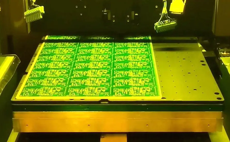
Lamination is the process of bonding the dry film solder mask to the PCB surface. This step is critical because improper lamination can lead to issues like air bubbles, uneven thickness, or poor adhesion, all of which compromise the board’s performance. The goal is to achieve a smooth, uniform layer that adheres tightly to the copper-clad substrate without defects.
There are two primary lamination techniques used in PCB manufacturing for applying dry film solder mask: vacuum lamination and hot roll lamination. Each method has unique advantages and is chosen based on the specific requirements of the board design, such as complexity, thickness, and production volume. Let’s break down these techniques to understand their processes, benefits, and ideal applications.
Vacuum Lamination: Precision for Complex Designs
Vacuum lamination is a widely used technique in modern PCB manufacturing, especially for multilayer boards and designs with strict impedance control. This method involves placing the PCB and dry film solder mask in a vacuum chamber to remove air before applying heat and pressure to bond the film to the board.
The process starts by cleaning the PCB surface to remove contaminants like dust or oil that could interfere with adhesion. The dry film is then aligned over the board, and both are placed in the vacuum laminator. By creating a vacuum environment (typically below 10 mbar), trapped air is eliminated, ensuring the film conforms tightly to the board’s surface, even in areas with fine traces or vias. Heat (around 100-120°C) and pressure (approximately 3-5 kg/cm2) are applied for a set duration, usually 30-60 seconds, to complete the bonding.
The key advantage of vacuum lamination is its ability to achieve uniform dielectric thickness, which is critical for maintaining signal integrity in high-speed applications. For instance, in a multilayer PCB designed for 10 Gbps data rates, even a slight variation in solder mask thickness (e.g., ±0.1 mil) can affect impedance values, leading to signal loss. Vacuum lamination minimizes such risks, making it ideal for complex, high-precision projects.
Additionally, this technique reduces the likelihood of air bubbles or voids, which can cause defects during subsequent processes like exposure or development. It’s particularly effective for boards with irregular surfaces or high-density interconnects (HDI), where consistent film adhesion is challenging.
Hot Roll Lamination: Speed and Efficiency for Simpler Designs
Hot roll lamination is another popular method for applying dry film solder mask, often favored for simpler PCB designs or high-volume production. This technique uses heated rollers to press the dry film onto the PCB surface as the board passes through the machine, combining heat and mechanical pressure to ensure adhesion.
In this process, the PCB is first cleaned to remove any debris or oxidation. The dry film solder mask, with one protective layer removed, is then fed into the laminator alongside the board. The rollers, heated to temperatures between 90-110°C, apply consistent pressure (around 2-4 kg/cm2) to bond the film to the copper surface. The speed of the rollers can be adjusted based on the board’s material and thickness, typically ranging from 1 to 3 meters per minute for standard FR-4 substrates.
Hot roll lamination is valued for its speed and cost-effectiveness, making it suitable for large-scale manufacturing where time is a critical factor. It works well for single-sided or double-sided PCBs with standard trace widths (e.g., 6 mils or wider) and less stringent impedance requirements. However, it may not provide the same level of precision as vacuum lamination, especially on boards with fine features or uneven surfaces, where air entrapment or uneven pressure can lead to defects.
One limitation of hot roll lamination is the potential for wrinkles or misalignment if the film or board isn’t perfectly flat during processing. To mitigate this, manufacturers often use advanced equipment with precise tension control and alignment systems to ensure consistent results.
Comparing Vacuum Lamination and Hot Roll Lamination
Choosing between vacuum lamination and hot roll lamination depends on the specific needs of your PCB project. Let’s compare these two techniques based on key factors like precision, speed, cost, and application suitability.
- Precision: Vacuum lamination offers superior precision and uniformity, making it the go-to choice for multilayer and HDI boards. Hot roll lamination, while effective, may struggle with fine-pitch designs or irregular surfaces.
- Speed: Hot roll lamination is faster, allowing for higher throughput in production. It’s ideal for simpler designs where speed trumps ultra-fine accuracy. Vacuum lamination, due to its batch process nature, takes longer per board.
- Cost: Hot roll lamination is generally more cost-effective, especially for large runs, as it requires less complex equipment and setup. Vacuum lamination involves higher equipment costs and longer processing times, increasing expenses.
- Application Suitability: For high-frequency or high-speed designs (e.g., boards operating at 5 GHz or supporting 10 Gbps signals), vacuum lamination ensures consistent dielectric properties. Hot roll lamination suits standard applications like consumer electronics with less demanding performance needs.
Understanding these differences helps manufacturers select the right technique to balance quality and efficiency. At ALLPCB, we tailor our lamination approach based on the unique specifications of each project to deliver optimal results.
Steps in Dry Film Solder Mask Application Process
Beyond lamination, applying dry film solder mask involves several key steps to ensure the protective layer performs as intended. Here’s a detailed look at the typical workflow in PCB manufacturing:
- Surface Preparation: The PCB surface is cleaned using chemical or mechanical methods to remove contaminants like oil, dust, or oxidation. A clean surface is essential for strong film adhesion.
- Lamination: As discussed, the dry film is applied using either vacuum or hot roll lamination to bond it securely to the board.
- Exposure: The laminated board is exposed to UV light through a photomask, which defines the areas where the solder mask will remain. The photosensitive film hardens in exposed areas, while unexposed areas remain soluble.
- Development: The board is immersed in a developer solution (often sodium carbonate-based) to remove unexposed film, revealing the copper pads and traces where solder will be applied.
- Curing: The board undergoes a final heat treatment (typically at 150°C for 30-60 minutes) to fully cure the solder mask, enhancing its durability and resistance to soldering temperatures (up to 260°C during reflow).
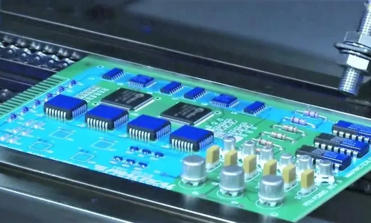
- Inspection: The board is inspected for defects like pinholes, misalignment, or uneven thickness using automated optical inspection (AOI) systems to ensure quality.
Each step requires precision to avoid issues like incomplete coverage or film delamination, which could lead to board failure during assembly or operation.
Benefits of Dry Film Solder Mask in PCB Manufacturing
Using dry film solder mask offers several advantages over other types like liquid photoimageable (LPI) masks, especially when paired with the right lamination technique. Here are some key benefits:
- Uniform Thickness: Dry film provides consistent thickness (typically 0.8-1.5 mils), crucial for impedance-controlled designs in high-speed circuits.
- High Resolution: It supports fine-pitch patterns, making it suitable for modern, compact PCB layouts with trace widths as narrow as 3 mils.
- Ease of Handling: Unlike liquid masks, dry film is easier to store and apply without the mess or risk of uneven coating.
- Durability: Once cured, it withstands harsh conditions like high temperatures and chemical exposure during soldering and assembly.
These benefits make dry film solder mask a preferred choice for many applications, from consumer electronics to industrial control systems.
Common Challenges and Solutions in Lamination Techniques
While lamination techniques like vacuum and hot roll are highly effective, they come with potential challenges. Here’s how manufacturers address common issues to ensure quality:
- Air Bubbles: Trapped air during lamination can create voids in the solder mask. Vacuum lamination inherently reduces this risk by removing air, while hot roll systems use precise roller pressure and tension control to minimize bubbles.
- Uneven Adhesion: Poor surface preparation or inconsistent pressure can lead to weak bonding. Thorough cleaning and calibrated equipment settings (e.g., maintaining roller pressure at 3 kg/cm2) help achieve uniform adhesion.
- Wrinkles or Misalignment: Especially in hot roll lamination, film wrinkles can occur if the board or film isn’t flat. Advanced laminators with automated alignment systems prevent this by ensuring precise positioning.
By addressing these challenges, manufacturers can maintain high standards in PCB production, ensuring reliability even in demanding applications.
Conclusion: Mastering Dry Film Solder Mask Application with ALLPCB
Dry film solder mask application is a cornerstone of PCB manufacturing, providing essential protection and precision for reliable circuit performance. Lamination techniques like vacuum lamination and hot roll lamination play a pivotal role in ensuring the film adheres uniformly and effectively to the board. While vacuum lamination excels in precision for complex, high-speed designs, hot roll lamination offers speed and efficiency for standard projects.
At ALLPCB, we leverage advanced equipment and expertise to apply dry film solder mask using the most suitable lamination method for your specific needs. Whether you’re designing a multilayer board for high-frequency applications or a simple double-sided PCB for consumer use, our tailored solutions ensure top-quality results every time.
Understanding these techniques empowers engineers and designers to make informed decisions, optimizing their PCB projects for performance and cost. With the right approach to dry film solder mask application, you can achieve durable, high-performing boards that meet the demands of today’s technology landscape.


