 ALLPCB


Introduction
High-speed memory interfaces like DDR4 push the boundaries of PCB design, where signal integrity hinges on meticulous differential pair routing. As clock rates exceed 1600 MHz and data transfers reach multi-gigabit speeds, even minor routing imperfections can degrade performance through reflections, crosstalk, or timing errors. Electric engineers must prioritize ddr4 differential pair strategies to ensure reliable memory interfaces in applications from servers to embedded systems. This article breaks down the core principles, best practices, and evolving challenges for DDR4 and newer standards like DDR5. By focusing on structured pcb design techniques, designers can mitigate signal integrity risks and achieve robust high-speed memory operation. Understanding these elements enables teams to deliver boards that meet stringent timing and eye diagram requirements.
What Are Differential Pairs and Why Do They Matter in High-Speed Memory Interfaces?
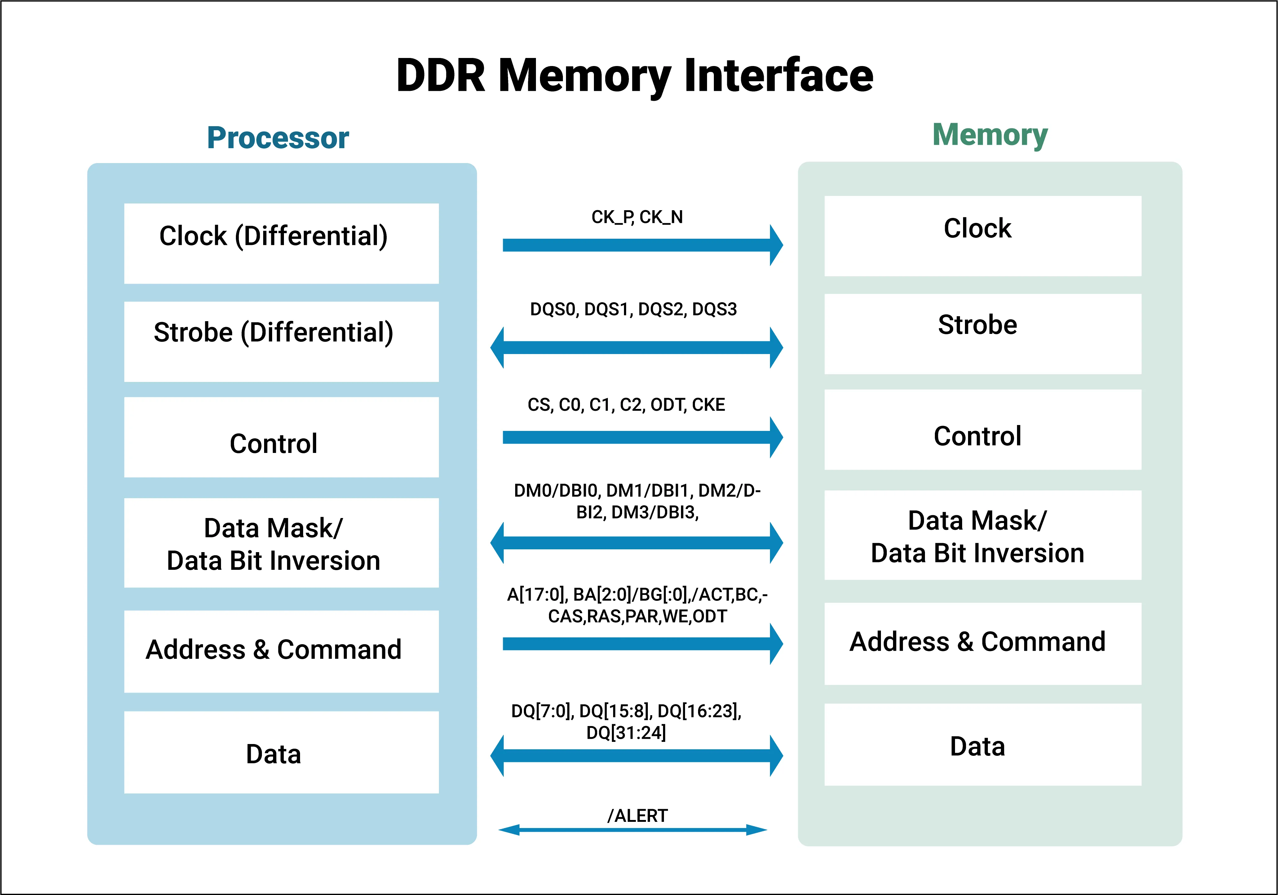
Differential pairs consist of two closely coupled traces that carry complementary signals, typically equal in magnitude but opposite in polarity. In DDR4 memory interfaces, these pairs primarily handle clock (CK/CK#) and data strobe (DQS/DQS#) signals, as defined in JEDEC JESD79-4. The differential signaling rejects common-mode noise, preserves signal integrity over long traces, and supports high data rates essential for modern computing. Without proper differential pair routing, high-speed memory systems suffer from increased bit error rates, reduced eye opening, and failure to meet setup and hold times. For electric engineers, mastering ddr4 differential pair implementation directly impacts system reliability in dense, multi-layer PCBs. This approach becomes even more critical as interfaces scale to DDR5, with doubled bandwidth and tighter margins.
Differential pairs matter because they convert single-ended noise sources into differential mode conversions only under imbalance conditions. In pcb design for high-speed memory, maintaining pair symmetry minimizes intra-pair skew, ensuring the receiver detects the voltage difference accurately. Poor routing leads to electromagnetic interference that propagates as jitter, compounding with process variations. Engineers must consider these factors early in the layout phase to avoid costly respins. Ultimately, differential pairs enable the transition from legacy single-ended signaling to robust, noise-immune architectures.
Technical Principles of Differential Pair Routing for Signal Integrity
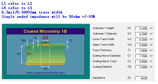
The foundation of differential pair routing lies in controlled impedance, where the pair maintains a characteristic differential impedance, often targeted at 100 ohms for DDR4 signals. This requires precise trace width, spacing, and reference plane proximity, calculated via stackup models to account for dielectric constants. Length matching within the pair prevents skew; typical tolerances demand less than 5 mils difference to keep propagation delays synchronized. Crosstalk arises from capacitive and inductive coupling, so spacing rules like 3 times the trace width (3W) from adjacent signals are standard to isolate high-speed memory nets. Vias introduce discontinuities, demanding back-drilling or stub minimization to preserve signal integrity.
Routing geometry plays a pivotal role in mode conversion, where bends or asymmetries convert differential signals to common-mode, amplifying noise. Engineers route pairs edge-coupled on the same layer, using 45-degree or curved bends with equal radii for both traces. Per IPC-2221 guidelines, high-speed signals avoid splits in reference planes to ensure continuous return paths, reducing ground bounce. For DDR4 fly-by topologies, address and command buses fan out with controlled skew budgets across ranks. These principles extend to DDR5, where per-lane decision feedback equalization demands even tighter control over pair integrity.
Propagation delay uniformity across the memory interface requires group length matching, such as aligning DQS to its DQ group within 50 mils. Reflections from impedance mismatches cause overshoot and ringing, analyzed via time-domain reflectometry in simulations. Dielectric losses increase with frequency, favoring low-loss materials for traces longer than 10 inches. Thermal expansion mismatches can warp pairs post-fabrication, underscoring the need for symmetric routing layers. Mastering these mechanisms ensures ddr4 differential pair performance scales reliably.
Best Practices for Differential Pair Routing in PCB Design
Start with stackup planning: dedicate inner layers for high-speed memory signals with adjacent solid ground planes for return currents. Target 50-ohm single-ended and 100-ohm differential impedance with +/-10% tolerance, verified through field solver tools during design. Route ddr4 differential pairs as straight as possible, minimizing vias and using blind/buried types where necessary to reduce stub lengths below 20 mils. Implement length tuning with serpentine patterns, ensuring no acute angles sharper than 135 degrees to avoid radiation. Maintain 5W spacing from non-related nets and shield clocks with ground traces if routing near sensitive analog sections.
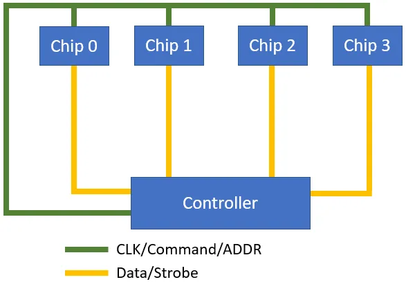
For fly-by DDR4 routing, position the memory controller centrally to equalize branch lengths, with write leveling calibration handling per-DIMM skew. Avoid routing under large power planes or crystals to prevent coupling. In multi-rank configurations, compensate for rank-to-rank delays using fly-by stubs under 200 mils. Transitioning to DDR5 introduces two independent 32-bit channels per DIMM, doubling differential pair density and requiring on-die termination (ODT) optimization. Pre-layout simulations predict eye diagrams, guiding iterative routing refinements.
Layer sequencing enforces orthogonal routing: horizontal pairs on one layer, vertical on adjacent to minimize broadside coupling. Fanout strategies prioritize inner layers for length-critical nets, reserving outer layers for lower-speed signals. Post-routing, perform design rule checks for skew, impedance deviations, and plane clearance. Fabrication notes specify controlled impedance testing per IPC standards. These practices ensure signal integrity across high-speed memory interfaces.
Troubleshooting Signal Integrity Issues in High-Speed Memory Routing
Engineers often encounter eye closure from excessive intra-pair skew, diagnosed via oscilloscope captures at the receiver. Simulate with IBIS models to isolate routing versus driver contributions. Crosstalk manifests as glitches on quiet lines; increase spacing or add ground shielding to resolve. Reflections appear as ringing; check for unterminated ends or via stubs exceeding quarter-wavelength at the frequency of interest.
For DDR4, write timing failures point to DQS-DQ misalignment, addressed by re-tuning lengths within groups. DDR5 adds decision feedback challenges, requiring per-lane equalization settings. Thermal simulations predict warpage effects on pair alignment. Systematic DRC automation catches 80% of issues pre-spin. Field returns highlight via resonance; mitigate with stitching capacitors.
Conclusion
Differential pair routing forms the backbone of reliable high-speed memory interfaces, from DDR4's foundational specs to DDR5's advanced demands. Key principles like impedance control, length matching, and crosstalk mitigation, combined with structured pcb design practices, safeguard signal integrity. Electric engineers benefit from early simulation, disciplined stackups, and adherence to standards like JEDEC JESD79-4 and IPC-2221. As speeds rise, these techniques evolve but remain essential for minimizing errors and maximizing throughput. Implementing them proactively reduces design cycles and enhances system performance.
FAQs
Q1: What is the typical differential impedance for a ddr4 differential pair in memory interfaces?
A1: In DDR4 pcb design, differential pairs for DQS and CK signals target 100 ohms, with single-ended traces at 50 ohms. This ensures matched transmission lines that preserve signal integrity at data rates up to 3200 MT/s. Tolerance stays within +/-10%, verified via TDR measurements during fabrication. Proper stackup planning achieves this without excessive trace widths.
Q2: How does length matching impact signal integrity in high-speed memory routing?
A2: Length matching in ddr4 differential pair routing keeps intra-pair skew below 5 mils, preventing timing errors at the receiver. Group matching aligns DQS to DQ lanes within 50 mils for fly-by topologies. Violations cause jitter accumulation, closing eye diagrams. Use serpentine tuning cautiously to avoid added inductance.
Q3: What spacing rules apply to differential pairs in high-speed memory pcb design?
A3: Maintain 3W to 5W spacing between ddr4 differential pairs and adjacent signals to minimize crosstalk. Pairs route parallel on the same layer with tight coupling (4-6 mil gap). Orthogonal layering reduces broadside coupling. This preserves noise margins in dense memory interfaces.
Q4: Why is reference plane continuity critical for memory interface differential pairs?
A4: Continuous ground planes under differential pairs provide low-impedance return paths, reducing EMI and ground bounce in high-speed memory. Splits force detours, increasing inductance and reflections. Stitch planes with vias near splits. This upholds signal integrity per IPC guidelines.
References
JEDEC JESD79-4 — DDR4 SDRAM Standard. JEDEC.
IPC-2221B — Generic Standard on Printed Board Design. IPC.
IPC-6012E — Qualification and Performance Specification for Rigid Printed Boards. IPC, 2018.


