If you're looking for ways to design PCBs for easy through-hole assembly, you're in the right place. Through-hole technology remains a go-to choice for many applications due to its durability and reliability, especially in high-stress or high-power environments. To ensure smooth assembly and optimal performance, you need to follow specific design practices. In this comprehensive guide, we'll cover through-hole PCB layout guidelines, through-hole component spacing, through-hole pad design, thermal management for through-hole, and drill size for through-hole components. Let's dive into the details to help you create robust and assembly-friendly PCB designs.
Why Through-Hole Assembly Still Matters
Through-hole technology (THT) involves inserting component leads into drilled holes on a PCB and soldering them on the opposite side. Despite the rise of surface-mount technology (SMT), THT is still widely used for components that require strong mechanical connections, such as connectors, transformers, and high-power resistors. Its advantages include better durability under vibration and thermal stress, making it ideal for automotive, industrial, and military applications. However, designing for THT assembly requires careful planning to avoid issues during manufacturing and soldering. Let's explore the best practices to make this process seamless.
Key Through-Hole PCB Layout Guidelines
Creating a PCB layout optimized for through-hole assembly starts with understanding the fundamental rules. These guidelines ensure that components fit correctly, soldering is efficient, and the board performs reliably.
- Component Orientation: Align components in a uniform direction whenever possible. For example, place resistors and capacitors with their leads oriented in the same direction to simplify manual or automated insertion during assembly. This reduces errors and speeds up the process.
- Grid-Based Placement: Use a grid system (e.g., 0.1-inch spacing) to position through-hole components. This standard spacing matches most component lead pitches and helps maintain consistency across the board.
- Clearance Around Holes: Ensure there’s enough space around each drilled hole to avoid interference with nearby traces or components. A minimum clearance of 0.010 inches (0.25 mm) between the edge of the hole and any copper trace is often recommended.
- Trace Routing: Keep traces away from through-hole pads to prevent accidental shorts during soldering. Route traces between pads only if necessary, and use a minimum trace width of 0.008 inches (0.2 mm) for standard current loads.
Through-Hole Component Spacing: Getting It Right
Proper spacing between through-hole components is critical for easy assembly and reliable performance. Insufficient spacing can lead to soldering defects, while excessive spacing wastes valuable board real estate. Here are some tips for optimizing through-hole component spacing:
- Minimum Spacing: Maintain at least 0.100 inches (2.54 mm) between the bodies of adjacent through-hole components. This prevents interference during insertion and allows room for soldering tools.
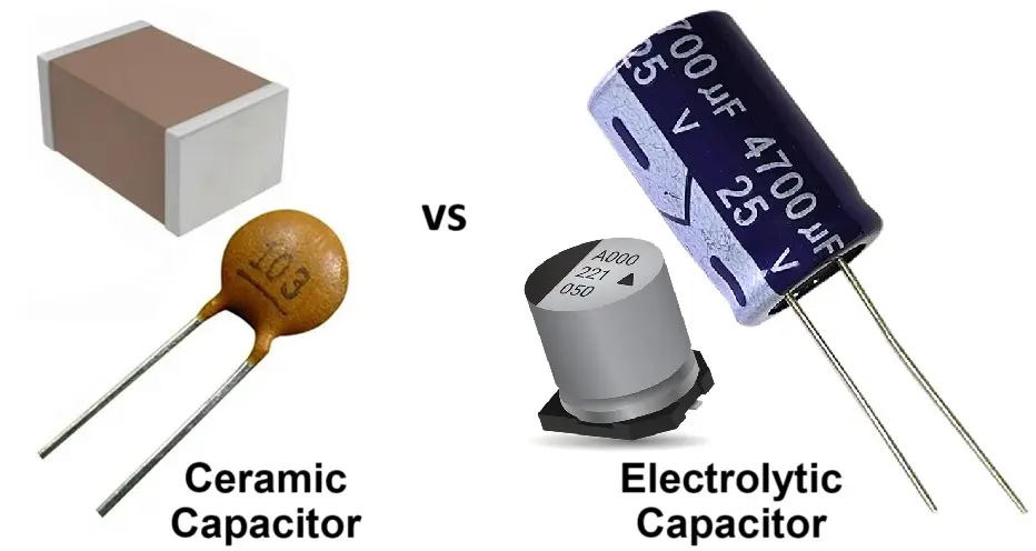
- Height Consideration: For taller components like electrolytic capacitors, increase spacing to 0.150 inches (3.81 mm) or more to avoid mechanical stress or shadowing during wave soldering.
- Automated Assembly: If using automated insertion equipment, check the machine’s spacing requirements. Many machines need a minimum of 0.120 inches (3 mm) between components for accurate placement.
- Board Edge Clearance: Keep components at least 0.200 inches (5 mm) away from the board’s edge to prevent damage during handling or depaneling.
By adhering to these spacing rules, you can reduce assembly errors and improve the overall manufacturability of your PCB design.
Through-Hole Pad Design: Ensuring Strong Connections
The design of pads for through-hole components directly impacts the quality of solder joints and the mechanical strength of the assembly. Poor through-hole pad design can lead to weak connections or manufacturing defects. Follow these best practices:
- Annular Ring Size: The annular ring (the copper area surrounding the drilled hole) should be at least 0.010 inches (0.25 mm) wide on each side of the hole. This ensures enough copper for a strong solder joint. For high-reliability applications, consider increasing this to 0.015 inches (0.38 mm).
- Pad Diameter: The pad diameter should be 1.5 to 2 times the diameter of the drilled hole. For a 0.040-inch (1 mm) hole, a pad diameter of 0.060 to 0.080 inches (1.5 to 2 mm) is ideal.
- Thermal Reliefs: Use thermal relief patterns (spokes connecting the pad to a plane) for pads connected to large copper planes. This prevents heat dissipation issues during soldering. A typical thermal relief spoke width is 0.010 inches (0.25 mm).
- Solder Mask Clearance: Ensure the solder mask opening around the pad is at least 0.004 inches (0.1 mm) larger than the pad itself to avoid mask overlap, which can interfere with soldering.
Proper pad design not only facilitates assembly but also enhances the long-term reliability of the PCB by ensuring robust solder joints.
Thermal Management for Through-Hole Components
Effective thermal management for through-hole designs is essential, especially for components that handle high power or operate in harsh environments. Without proper heat dissipation, components can overheat, leading to failure or reduced lifespan. Here are some strategies to manage heat:
- Use of Thermal Pads: For power components like transistors or voltage regulators, connect through-hole pads to large copper areas or planes to act as heat sinks. Ensure the copper area is at least 0.5 square inches (3.2 square cm) per watt of power dissipated.
- Thermal Vias: Place thermal vias (small plated-through holes) around high-heat components to transfer heat to the opposite side of the board or to an internal ground plane. A grid of 0.012-inch (0.3 mm) vias spaced 0.050 inches (1.27 mm) apart works well for most designs.
- Component Placement: Position heat-generating components away from sensitive parts like microcontrollers. Allow at least 0.200 inches (5 mm) of spacing between high-heat and low-heat components to minimize thermal interference.
- Board Thickness: For high-power applications, consider using a thicker PCB (e.g., 0.093 inches or 2.36 mm) to improve heat dissipation through the board material.
By incorporating these thermal management techniques, you can protect your through-hole components from overheating and ensure consistent performance.
Choosing the Right Drill Size for Through-Hole Components
Selecting the correct drill size for through-hole components is crucial for proper fit and reliable soldering. If the hole is too small, the component lead won’t fit; if it’s too large, the solder joint may be weak. Follow these guidelines to get it right:
- Hole Diameter: The drilled hole should be 0.004 to 0.008 inches (0.1 to 0.2 mm) larger than the component lead diameter. For example, a lead with a diameter of 0.032 inches (0.81 mm) should have a hole size of 0.036 to 0.040 inches (0.91 to 1.02 mm).
- Standard Sizes: Stick to standard drill sizes to avoid custom tooling costs. Common sizes include 0.028 inches (0.71 mm) for small leads and 0.040 inches (1.02 mm) for larger leads like those on connectors.
- Tolerance: Account for manufacturing tolerances in drill size, typically ±0.002 inches (0.05 mm). Consult with your PCB manufacturer to confirm their capabilities.
- Aspect Ratio: For thicker boards, ensure the hole’s aspect ratio (board thickness to hole diameter) does not exceed 10:1 to avoid drilling issues. For a 0.062-inch (1.57 mm) thick board, the smallest hole should be at least 0.006 inches (0.15 mm) in diameter.
Choosing the right drill size ensures that components are securely placed and soldered without risking damage to the board or leads.
Additional Tips for Easy Through-Hole Assembly
Beyond the core design aspects, a few extra tips can make through-hole assembly even smoother:
- Silkscreen Markings: Clearly label component positions and polarities on the silkscreen layer. For example, mark the positive lead of a capacitor with a “+” symbol to prevent incorrect insertion.
- Test Points: Include test points near through-hole components for easy debugging after assembly. A test point pad of 0.040 inches (1 mm) in diameter is usually sufficient.
- Tooling Holes: Add non-plated tooling holes (e.g., 0.125 inches or 3.175 mm in diameter) at the board corners for alignment during assembly. Place them at least 0.150 inches (3.81 mm) from any components or traces.
- Soldering Method: Design with the soldering method in mind. For wave soldering, ensure components are placed on the top side with leads protruding to the bottom. For hand soldering, leave extra space around pads for easy access.
These small considerations can save significant time and effort during the assembly process, ensuring a high-quality final product.
Common Mistakes to Avoid in Through-Hole PCB Design
Even with the best intentions, certain design errors can complicate through-hole assembly. Here are some pitfalls to watch out for:
- Inadequate Pad Size: Designing pads that are too small can result in weak solder joints. Always follow the recommended annular ring and pad diameter guidelines.
- Overcrowding Components: Placing components too close together can make insertion and soldering difficult, especially for manual assembly.
- Ignoring Thermal Needs: Failing to account for heat dissipation can lead to component failure. Always include thermal reliefs or vias for high-power parts.
- Incorrect Drill Sizes: Using a drill size that doesn’t match the lead diameter can cause fitment issues or poor connections.
By double-checking your design against these common mistakes, you can avoid costly rework and delays in production.
Conclusion: Mastering Through-Hole PCB Design
Designing PCBs for easy through-hole assembly requires attention to detail and adherence to proven best practices. By following through-hole PCB layout guidelines, optimizing through-hole component spacing, refining through-hole pad design, prioritizing thermal management for through-hole, and selecting the correct drill size for through-hole components, you can create boards that are not only easy to assemble but also reliable in operation. Whether you're working on a small prototype or a large-scale production run, these tips will help streamline the process and ensure high-quality results. Start applying these strategies in your next project to see the difference in assembly efficiency and performance.
 ALLPCB


