 ALLPCB


This article summarizes practical derating guidelines for power supply components. If a component operates within the supplier's specified limits, it can achieve its full lifetime. Derating is used to improve product reliability.
Derating rules are established based on worst-case operating conditions. Components operating under the worst-case conditions are major factors causing actual lifetimes to fall short of rated lifetimes.
Worst-case conditions are those in which a component is subjected to its maximum stresses. These conditions are typically a combination of external environmental parameters such as temperature, voltage, number of switching cycles, and load. Boundary conditions for these stresses are generally provided in component datasheets.
A robust design should assess reliability based on a component's design risk under worst-case conditions. Risk assessment identifies failure causes, potential hazards, probability of failure, and severity of consequences.
To establish derating specifications, perform failure risk assessment under worst-case conditions. Risk assessment requires building accelerated test models; performing assessments using normal-use times would be impractical for time-to-market.
Model accuracy strongly affects risk assessment results. Ensuring model accuracy is complex; this article provides a qualitative overview.
Accelerated Test Models
Acceleration factors in accelerated tests often follow the Arrhenius law.
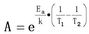
Where:
- A: acceleration factor
- Ea: activation energy
- K: Boltzmann constant, 8.63E-5 eV/K
- T: absolute temperature
If the acceleration factor for a given derating condition is known, use the following relation to compute lifetimes under other conditions.
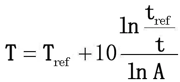
Where:
- T: temperature in degrees C
- Tref: reference derating temperature in degrees C
- tref: reference service life, unit kHrs
- t: service life, unit kHrs
- A: acceleration factor per 10 degrees C
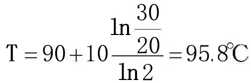
Example:
A component has a lifetime of 30 kHrs at 90°C, with an acceleration factor A approximately 2 per 10°C. At what temperature does the component lifetime become 20 kHrs?
1. Integrated Circuits
Due to IC complexity and confidentiality, reliability is generally inferred from semiconductor junction temperature.
Common guidelines:
- Maximum operating voltage should not exceed 80% of rated voltage.
- Maximum output current should not exceed 75% of rated current.
- Junction temperature should be at most 85°C, or not exceed 80% of the rated maximum junction temperature.
2. Diodes
Diode types vary widely, so there are general requirements and specific ones.
General requirements:
- Long-term reverse voltage: less than about 70%–90% of VRRM (maximum repetitive reverse voltage).
- Peak reverse voltage: less than 90% of VRRM.
- Average forward current: less than about 70%–90% of rated value.
- Forward peak current: less than 75%–85% of IFRM (forward repetitive peak current).
Operating junction temperature varies by diode type:
- Signal diodes: up to 85–150°C
- Glass-passivated diodes: up to 85–150°C
- Rectifier, fast recovery, ultra-fast recovery diodes (<1000 V): up to 85–125°C
- Rectifier, fast recovery, ultra-fast recovery diodes (≥1000 V): up to 85–115°C
- Schottky diodes: up to 85–115°C
- Zener diodes (<0.5 W): up to 85–125°C
- Zener diodes (≥0.5 W): up to 85–100°C
Reference empirical value for case temperature:
Tcase ≤ 0.8 × Tjmax - 2 × θjc × P, with 2 × θjc × P < 15°C. θjc is junction-to-case thermal resistance and P is power dissipation.
Many ranges are provided because reliability requirements and cost trade off; both conservative and cost-conscious ranges are given for reference.
3. Power MOSFETs
- VGS < 85% × VGSmax (maximum gate drive voltage)
- ID_peak < 80% × ID_M (maximum drain pulse current)
- VDS < 80%–90% × rated voltage
- dV/dt < 50%–90% × rated value
- Junction temperature: < 85°C or < 80% × Tjmax (maximum junction temperature)
Reference empirical value for case temperature:
Tcase ≤ 0.8 × Tjmax - 2 × θjc × P, with 2 × θjc × P < 15°C. θjc is junction-to-case thermal resistance and P is power dissipation.
4. Bipolar Transistors
- All voltage ratings should be limited to below 85% of rated values.
- Power dissipation should not exceed 70%–90% of rated value.
- IC must be derated by 30% in both RBSOA (reverse bias safe operating area) and FBSOA (forward bias safe operating area), i.e., operate at 70% of rated.
- Junction temperature should not exceed 85–125°C.
Reference empirical value for case temperature:
Tcase ≤ 0.75 × Tjmax - 2 × θjc × P, with 2 × θjc × P < 15°C. θjc is junction-to-case thermal resistance and P is power dissipation.
5. Electrolytic Capacitors (Aluminum)
Aluminum electrolytic capacitors are critical in switch-mode power supplies; many failures are caused by improper use. Because of their importance, more detailed rules are provided.
- Vdc + Vripple should be less than 90% of rated voltage.
- Avoid routing traces other than ground under the capacitor on the PCB front side.
- Ripple current is complex because switch-mode supplies have rich ripple spectra; convert ripple current using frequency factors provided by the supplier.
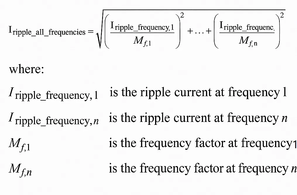
Frequency factors should be provided by suppliers.
Ripple current must be within about 70%–90% of the supplier's rated value.
- Initial capacitance should include a 20% margin. Also provide an additional 20% capacitance margin to accommodate end-of-life capacitance loss.
- Electrolytic capacitor lifetime temperature acceleration factor is about 2 per 10°C; that is, lifetime halves for each 10°C increase.
- Case temperature Tcase should be limited according to design life.
- Self-heating < 5°C. Self-heating refers to temperature rise caused solely by the capacitor's internal heating during operation.
6. Ceramic Capacitors
Operating voltage: less than about 60%–90% of rated voltage.
Surface temperature < 105°C.
Self-heating < 15°C or as defined in the datasheet, whichever is lower.
7. Film Capacitors
Do not use polystyrene capacitors in switch-mode power supplies because of their poor heat resistance.
Surface temperature < 85°C. If above 85°C, derate voltage as shown below. Voltage here refers to DC voltage plus AC peak voltage.
Polyester capacitor self-heating < 8°C or as defined in the datasheet, whichever is lower.
Polypropylene capacitor self-heating < 5°C or as defined in the datasheet, whichever is lower.
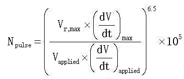
Film capacitor lifetime depends on voltage magnitude and pulse rise rate. The allowable number of pulses relates to voltage, pulse count, and dv/dt as follows.
Where:
- Npulse: total number of pulses
- Vr,max: maximum rated DC voltage
- Vapplied: actual applied peak-to-peak voltage
- (dv/dt)max: maximum rated pulse slope
- (dv/dt)applied: actual applied pulse slope
8. Resistors
Resistors are classified as fixed linear, fixed nonlinear, and variable.
Fixed linear types include carbon film, metal film, metal oxide film, metal glaze, carbon composition, and wirewound resistors.
Fixed nonlinear types include NTC and PTC devices.
Resistor reliability mainly depends on temperature, which is the sum of ambient temperature and self-heating from power dissipation.
Power and voltage both limit resistor selection and use.
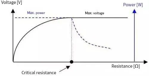
From the figure, resistors with values below a critical resistance are power-limited, while those above the critical resistance are voltage-limited.
Single-pulse power limits depend on pulse shape. Pulse peak voltage must not exceed rated limits.
Resistor derating rules:
- Use metal glaze resistors in circuits with transient high-voltage pulses.
- Use wirewound resistors where large surge currents occur.
- Continuous power < 50% of rated power.
- Avoid carbon film resistors > 1 MΩ due to poor long-term stability.
- High-value resistors with good long-term stability should be metal glaze types.
- After thermal shock testing, resistor value must remain within ±5% of rated value.
- Fuse resistors or fusible resistors should not be placed too close to the PCB to avoid overheating the board.
- Avoid using rectangular chip resistors in ESD protection circuits, as sharp corners can promote discharge.
- For voltage or current sensing, prefer chip resistor sizes 1206 or larger when possible.
- Derating for voltage withstand:
For carbon film, metal film, and metal oxide film resistors:
If R > 100 kΩ, VRMS < 50% of rated maximum continuous working voltage.
If R ≤ 100 kΩ, VRMS < 90% of rated maximum continuous working voltage or < 90% × (P × R)^0.5, whichever is lower.
For carbon composition, metal glaze, and wirewound resistors:
VRMS < 90% of rated maximum continuous working voltage or < 90% × (P × R)^0.5, whichever is lower.
9. Magnetic Components
Maximum voltages between windings or between winding and core should not exceed the limits shown below.
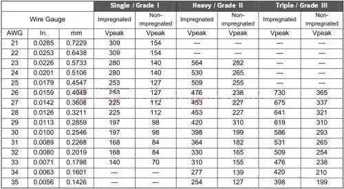
Convert AWG gauge to diameter in mm using: d = 25.4 × 0.005 × 92^((36 - AWG)/39).
Enamelled wire lifetime acceleration factor is about 2.5 per 10°C.
Wire insulation temperature derating:
- CLASS B: 95°C–110°C. Note: rated temperature is 130°C.
- CLASS F: 110°C–125°C. Note: rated temperature is 155°C.
- CLASS H: 125°C–150°C. Note: rated temperature is 180°C.
Core derating:
- Bmax < 80% of Bsat under all conditions, where Bsat is the core saturation flux density.
- Tcore < 70% of Tcurie - 10°C, where Tcurie is the material Curie temperature.
10. Metal Oxide Varistors (MOV)
Tcase ≤ 85°C under all conditions. Typical selection recommendations:
- AC 120 V / 127 V: choose 150 Vrms
- AC 220 V: choose 275 Vrms (this item can be debated)
- AC 277 V: choose 320 Vrms
- AC 347 V: choose 420 Vrms
11. Printed Circuit Boards
PCB materials and maximum usable surface temperatures:
- FR2: 75°C
- FR3: 90°C
- FR4: 125°C
- CEM1: 125°C
- CEM3: 125°C
Additional rules:
- Vias can be used to help heat dissipation.
- Current per via should not exceed 2 A.
- Spacing between traces versus voltage should follow UL 935 reference.
- FR1 thermal conductivity is about twice that of FR4, but FR1 is not suitable for double-sided boards.
12. Fuses
Derating fuses balances circuit protection reliability and fuse life; derating fuses does not directly improve product reliability.
Ambient temperature and current are the main factors affecting fuse life.
At 25°C, fuse current should be derated by 25%. With increasing ambient temperature, slow-blow fuses require an additional derating of about 0.5% per °C, while fast-acting fuses require about 0.1% per °C.
13. Optocouplers
- Maximum operating voltage: less than about 70%–90% of rated voltage.
- Maximum operating current: less than about 25%–90% of rated current.
- Current transfer ratio: retain a 20% margin for product life degradation.
- Junction temperature: < 85°C–100°C.
Derating practices are empirical and intended as practical guidance.


