ALLPCB


1. Clock-gating overview
In ASIC design, projects often expect code to be written in a clock-gating style so that during DC synthesis the registers can be synthesized into clock-gating structures to reduce switching power. When the control signal (vld_in) is inactive, registers with clock gating have their CK (clk) input held at 0, so they do not toggle. This reduces register switching power and the switching power in the clock tree.
As shown below: the left diagram is the clock-gating structure after DC synthesis, using an integrated clock-gating cell to gate the clock; the gated clock is connected to the register CK pins.
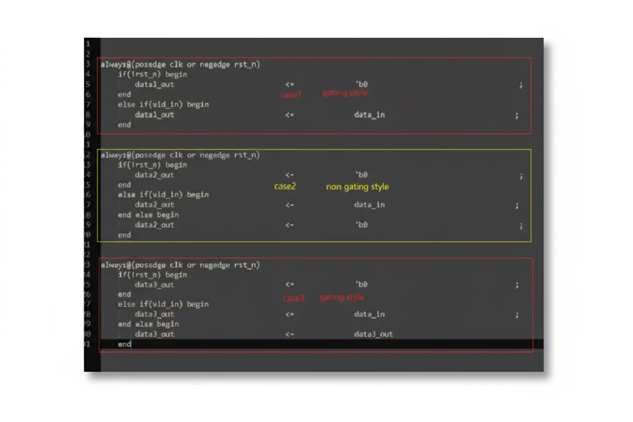
2. Clock-gating coding styles
As shown below, case 1 and case 3 follow a gating-style pattern. DC synthesis is more likely to generate clock gating for these styles. NO TE: this means "more likely", not guaranteed. The synthesis tool makes decisions based on the number of register bits that share the same vld control; if the number is too small, the tool may not apply clock gating because the ICG cell itself adds area and leakage/power overhead.
In case 1 the data width is 3 bits, so clock gating was not generated.
In case 2 the data width is 7 bits, and both data1_out and data3_out generated clock gating.
3. Data width: 3 bits
3.1 RTL code
module try_top (
    input                                               clk                                    ,   //
    input                                               rst_n                                  ,   //
    input                                               vld_in                                 ,   //
    input               [3-1:0]                        data_in                                ,   //
    output  reg                                         vld_out                                ,   //
    output  reg         [3-1:0]                        data3_out                               ,   //
    output  reg         [3-1:0]                        data1_out                               ,   //
    output  reg         [3-1:0]                        data2_out                                   //
);
always@(posedge clk or negedge rst_n)
    if(!rst_n) begin
        vld_out                          <=              1'b0                                    ;
    end
    else begin
        vld_out                          <=              vld_in                                  ;
    end
always@(posedge clk or negedge rst_n)
    if(!rst_n) begin
        data1_out                          <=              'b0                                    ;
    end
    else if(vld_in) begin
        data1_out                          <=              data_in                               ;
    end
always@(posedge clk or negedge rst_n)
    if(!rst_n) begin
        data2_out                          <=              'b0                                    ;
    end
    else if(vld_in) begin
        data2_out                          <=              data_in                               ;
    end else begin
        data2_out                          <=              'b0                                    ;
    end
always@(posedge clk or negedge rst_n)
    if(!rst_n) begin
        data3_out                          <=              'b0                                   ;
    end
    else if(vld_in) begin
        data3_out                          <=              data_in                               ;
    end else begin
        data3_out                          <=              data3_out                             ;
    end
    endmodule
3.2 Synthesized netlist — no clock gating generated
module try_top ( clk, rst_n, vld_in, data_in, vld_out, data3_out, data1_out,
        data2_out );
  input [2:0] data_in;
  output [2:0] data3_out;
  output [2:0] data1_out;
  output [2:0] data2_out;
  input clk, rst_n, vld_in;
  output vld_out;
  wire   n6, n8, n10, n12, n14, n16, n18, n20, n22, n24, n26;
  SDFFRPQL_*CELL_TYPE* data2_out_reg_0_ ( .D(n6), .SI(1'b0), .SE(1'b0),
        .CK(clk), .R(n24), .Q(data2_out[0]) );
  SDFFRPQL_*CELL_TYPE* vld_out_reg ( .D(vld_in), .SI(1'b0), .SE(1'b0),
        .CK(clk), .R(n24), .Q(vld_out) );
  SDFFRPQL_*CELL_TYPE* data1_out_reg_2_ ( .D(n22), .SI(1'b0), .SE(1'b0),
        .CK(clk), .R(n24), .Q(data1_out[2]) );
  SDFFRPQL_*CELL_TYPE* data1_out_reg_1_ ( .D(n20), .SI(1'b0), .SE(1'b0),
        .CK(clk), .R(n24), .Q(data1_out[1]) );
  SDFFRPQL_*CELL_TYPE* data1_out_reg_0_ ( .D(n18), .SI(1'b0), .SE(1'b0),
        .CK(clk), .R(n24), .Q(data1_out[0]) );
  SDFFRPQL_*CELL_TYPE* data3_out_reg_2_ ( .D(n16), .SI(1'b0), .SE(1'b0),
        .CK(clk), .R(n24), .Q(data3_out[2]) );
  SDFFRPQL_*CELL_TYPE* data3_out_reg_1_ ( .D(n14), .SI(1'b0), .SE(1'b0),
        .CK(clk), .R(n24), .Q(data3_out[1]) );
  SDFFRPQL_*CELL_TYPE* data3_out_reg_0_ ( .D(n12), .SI(1'b0), .SE(1'b0),
        .CK(clk), .R(n24), .Q(data3_out[0]) );
  SDFFRPQL_*CELL_TYPE* data2_out_reg_2_ ( .D(n10), .SI(1'b0), .SE(1'b0),
        .CK(clk), .R(n24), .Q(data2_out[2]) );
  SDFFRPQL_*CELL_TYPE* data2_out_reg_1_ ( .D(n8), .SI(1'b0), .SE(1'b0),
        .CK(clk), .R(n24), .Q(data2_out[1]) );
  INVP_*CELL_TYPE* U18 ( .A(rst_n), .Y(n24) );
  AND2_*CELL_TYPE* U19 ( .A(data_in[1]), .B(vld_in), .Y(n8) );
  AND2_*CELL_TYPE* U20 ( .A(data_in[2]), .B(vld_in), .Y(n10) );
  AND2_*CELL_TYPE* U21 ( .A(data_in[0]), .B(vld_in), .Y(n6) );
  INVP_*CELL_TYPE* U22 ( .A(vld_in), .Y(n26););
  AO21_*CELL_TYPE* U23 ( .A0(data3_out[1]), .A1(n26), .B0(n8), .Y(n14););
  AO21_*CELL_TYPE* U24 ( .A0(data3_out[0]), .A1(n26), .B0(n6), .Y(n12););
  AO21_*CELL_TYPE* U25 ( .A0(data1_out[0]), .A1(n26), .B0(n6), .Y(n18););
  AO21_*CELL_TYPE* U26 ( .A0(data1_out[1]), .A1(n26), .B0(n8), .Y(n20););
  AO21_*CELL_TYPE* U27 ( .A0(data3_out[2]), .A1(n26), .B0(n10), .Y(n16);
  AO21_*CELL_TYPE* U28 ( .A0(data1_out[2]), .A1(n26), .B0(n10), .Y(n22);
endmodule
4. Data width: 7 bits
4.1 RTL code
module try_top (
    input                                               clk                                    ,   //
    input                                               rst_n                                  ,   //
    input                                               vld_in                                 ,   //
    input               [7-1:0]                        data_in                                ,   //
    output  reg                                         vld_out                                ,   //
    output  reg         [7-1:0]                        data3_out                               ,   //
    output  reg         [7-1:0]                        data1_out                               ,   //
    output  reg         [7-1:0]                        data2_out                                   //
);
always@(posedge clk or negedge rst_n)
    if(!rst_n) begin
        vld_out                          <=              1'b0                                    ;
    end
    else begin
        vld_out                          <=              vld_in                                  ;
    end
always@(posedge clk or negedge rst_n)
    if(!rst_n) begin
        data1_out                          <=              'b0                                    ;
    end
    else if(vld_in) begin
        data1_out                          <=              data_in                               ;
    end
always@(posedge clk or negedge rst_n)
    if(!rst_n) begin
        data2_out                          <=              'b0                                    ;
    end
    else if(vld_in) begin
        data2_out                          <=              data_in                               ;
    end else begin
        data2_out                          <=              'b0                                    ;
    end
always@(posedge clk or negedge rst_n)
    if(!rst_n) begin
        data3_out                          <=              'b0                                   ;
    end
    else if(vld_in) begin
        data3_out                          <=              data_in                               ;
    end else begin
        data3_out                          <=              data3_out                             ;
    end
    endmodule
4.2 Synthesized netlist — clock gating generated
module try_top ( clk, rst_n, vld_in, data_in, vld_out, data3_out, data1_out,
        data2_out );
  input [6:0] data_in;
  output [6:0] data3_out;
  output [6:0] data1_out;
  output [6:0] data2_out;
  input clk, rst_n, vld_in;
  output vld_out;
  wire   clk_gclk_0, n3, n5, n7, n9, n11, n13, n15, n31;
  SNPS_CLOCK_GATE_HIGH_try_top inferred_cg_0 ( .CLK(clk), .EN(vld_in), .ENCLK(
        clk_gclk_0), .TE(1'b0) );
  SDFFRPQL_*CELL_TYPE* data3_out_reg_0_ ( .D(data_in[0]), .SI(1'b0), .SE(
        1'b0), .CK(clk_gclk_0), .R(n31), .Q(data3_out[0]) );
  SDFFRPQL_*CELL_TYPE* data2_out_reg_0_ ( .D(n3), .SI(1'b0), .SE(1'b0),
        .CK(clk), .R(n31), .Q(data2_out[0]) );
  SDFFRPQL_*CELL_TYPE* vld_out_reg ( .D(vld_in), .SI(1'b0), .SE(1'b0),
        .CK(clk), .R(n31), .Q(vld_out) );
  SDFFRPQL_*CELL_TYPE* data1_out_reg_6_ ( .D(data_in[6]), .SI(1'b0), .SE(
        1'b0), .CK(clk_gclk_0), .R(n31), .Q(data1_out[6]) );
  SDFFRPQL_*CELL_TYPE* data1_out_reg_5_ ( .D(data_in[5]), .SI(1'b0), .SE(
        1'b0), .CK(clk_gclk_0), .R(n31), .Q(data1_out[5]) );
  SDFFRPQL_*CELL_TYPE* data1_out_reg_4_ ( .D(data_in[4]), .SI(1'b0), .SE(
        1'b0), .CK(clk_gclk_0), .R(n31), .Q(data1_out[4]) );
  SDFFRPQL_*CELL_TYPE* data1_out_reg_3_ ( .D(data_in[3]), .SI(1'b0), .SE(
        1'b0), .CK(clk_gclk_0), .R(n31), .Q(data1_out[3]) );
  SDFFRPQL_*CELL_TYPE* data1_out_reg_2_ ( .D(data_in[2]), .SI(1'b0), .SE(
        1'b0), .CK(clk_gclk_0), .R(n31), .Q(data1_out[2]) );
  SDFFRPQL_*CELL_TYPE* data1_out_reg_1_ ( .D(data_in[1]), .SI(1'b0), .SE(
        1'b0), .CK(clk_gclk_0), .R(n31), .Q(data1_out[1]) );
  SDFFRPQL_*CELL_TYPE* data1_out_reg_0_ ( .D(data_in[0]), .SI(1'b0), .SE(
        1'b0), .CK(clk_gclk_0), .R(n31), .Q(data1_out[0]) );
  SDFFRPQL_*CELL_TYPE* data3_out_reg_6_ ( .D(data_in[6]), .SI(1'b0), .SE(
        1'b0), .CK(clk_gclk_0), .R(n31), .Q(data3_out[6]) );
  SDFFRPQL_*CELL_TYPE* data3_out_reg_5_ ( .D(data_in[5]), .SI(1'b0), .SE(
        1'b0), .CK(clk_gclk_0), .R(n31), .Q(data3_out[5]) );
  SDFFRPQL_*CELL_TYPE* data3_out_reg_4_ ( .D(data_in[4]), .SI(1'b0), .SE(
        1'b0), .CK(clk_gclk_0), .R(n31), .Q(data3_out[4]) );
  SDFFRPQL_*CELL_TYPE* data3_out_reg_3_ ( .D(data_in[3]), .SI(1'b0), .SE(
        1'b0), .CK(clk_gclk_0), .R(n31), .Q(data3_out[3]) );
  SDFFRPQL_*CELL_TYPE* data3_out_reg_2_ ( .D(data_in[2]), .SI(1'b0), .SE(
        1'b0), .CK(clk_gclk_0), .R(n31), .Q(data3_out[2]) );
  SDFFRPQL_*CELL_TYPE* data3_out_reg_1_ ( .D(data_in[1]), .SI(1'b0), .SE(
        1'b0), .CK(clk_gclk_0), .R(n31), .Q(data3_out[1]) );
  SDFFRPQL_*CELL_TYPE* data2_out_reg_6_ ( .D(n15), .SI(1'b0), .SE(1'b0),
        .CK(clk), .R(n31), .Q(data2_out[6]) );
  SDFFRPQL_*CELL_TYPE* data2_out_reg_5_ ( .D(n13), .SI(1'b0), .SE(1'b0),
        .CK(clk), .R(n31), .Q(data2_out[5]) );
  SDFFRPQL_*CELL_TYPE* data2_out_reg_4_ ( .D(n11), .SI(1'b0), .SE(1'b0),
        .CK(clk), .R(n31), .Q(data2_out[4]) );
  SDFFRPQL_*CELL_TYPE* data2_out_reg_3_ ( .D(n9), .SI(1'b0), .SE(1'b0),
        .CK(clk), .R(n31), .Q(data2_out[3]) );
  SDFFRPQL_*CELL_TYPE* data2_out_reg_2_ ( .D(n7), .SI(1'b0), .SE(1'b0),
        .CK(clk), .R(n31), .Q(data2_out[2]) );
  SDFFRPQL_*CELL_TYPE* data2_out_reg_1_ ( .D(n5), .SI(1'b0), .SE(1'b0),
        .CK(clk), .R(n31), .Q(data2_out[1]) );
  INVP_*CELL_TYPE* U13 ( .A(rst_n), .Y(n31) );
  AND2_*CELL_TYPE* U14 ( .A(vld_in), .B(data_in[6]), .Y(n15) );
  AND2_*CELL_TYPE* U15 ( .A(vld_in), .B(data_in[5]), .Y(n13) );
  AND2_*CELL_TYPE* U16 ( .A(vld_in), .B(data_in[4]), .Y(n11) );
  AND2_*CELL_TYPE* U17 ( .A(vld_in), .B(data_in[3]), .Y(n9) );
  AND2_*CELL_TYPE* U18 ( .A(vld_in), .B(data_in[2]), .Y(n7) );
  AND2_*CELL_TYPE* U19 ( .A(vld_in), .B(data_in[1]), .Y(n5) );
  AND2_*CELL_TYPE* U20 ( .A(vld_in), .B(data_in[0]), .Y(n3) );
endmodule
5. ICG module description
ICG (integrated latch clock gate) is a clock-gating module that can disable the clock via an enable signal. Common uses include disabling parts of the clock tree in low-power states and glitch-free dynamic clock switching. The circuit below shows an example ICG structure: the input clock is CK, the gated output is ECK, and E is the enable. When E is 0 the clock is disabled and ECK output is 0.
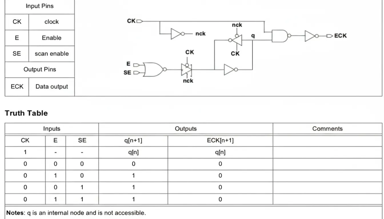
From the timing and structure: when CK is 0, ECK is held at 0 and the latch q follows E; if E is 1 then q is 1, if E is 0 then q is 0. When CK is 1, ECK holds the latched value q (the value of E sampled when CK was last 0). Therefore, if E is set to 0, ECK will transition to 0 at the falling edge of CK and remain 0 as long as E stays 0. When E changes from 0 to 1, ECK will switch to 1 at the next rising edge of CK.