ALLPCB


Introduction
High-frequency printed circuit boards (PCBs) are critical components in modern electronics, enabling the transmission of signals at elevated frequencies, typically above 100 MHz. These specialized boards are designed to handle rapid signal changes with minimal loss, making them indispensable in advanced technological fields. Their applications span across communication systems, radar systems, and medical equipment, where precision and reliability are paramount. For electrical engineers, understanding the role of high-frequency PCBs is essential to designing systems that meet stringent performance requirements. This article explores the diverse applications of these boards, delving into their technical principles and practical significance in various industries. By examining their use in cutting-edge technologies, we aim to provide insights into why high-frequency PCBs are vital for innovation and efficiency in electronic design.
What Are High-Frequency PCBs and Why Do They Matter?
High-frequency PCBs are engineered to operate at frequencies where standard boards fail to maintain signal integrity. These boards utilize specialized materials and design techniques to minimize signal loss and interference, ensuring efficient data transmission. Their importance lies in their ability to support applications requiring fast, accurate signal processing, such as wireless networks and imaging systems. In industries like telecommunications, defense, and healthcare, high-frequency PCBs enable devices to perform under demanding conditions. For electrical engineers, selecting the right materials and configurations for these boards directly impacts system performance. Without such specialized designs, modern technologies like 5G networks or advanced diagnostic tools would struggle to function effectively. Thus, high-frequency PCBs are foundational to pushing the boundaries of electronic capabilities across multiple sectors.
Technical Principles Behind High-Frequency PCBs
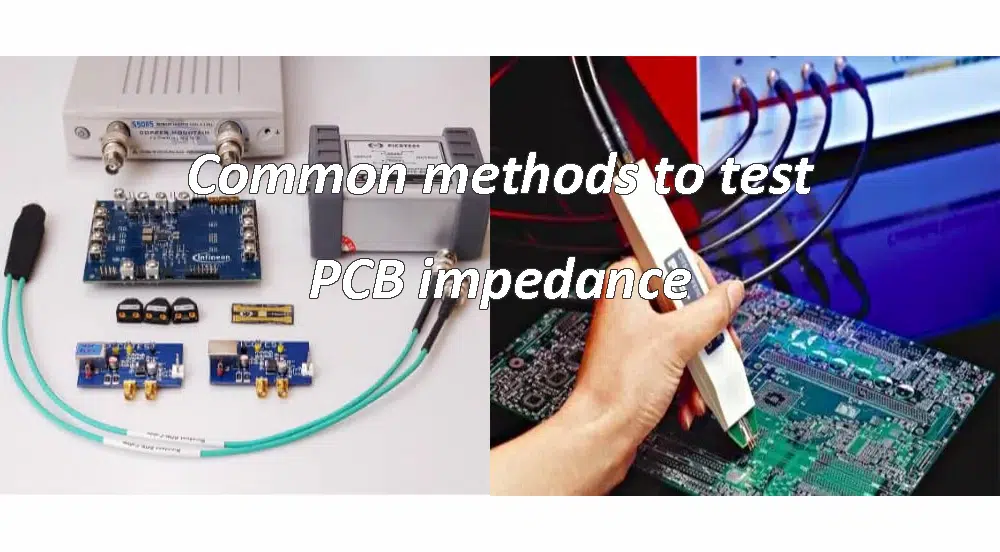
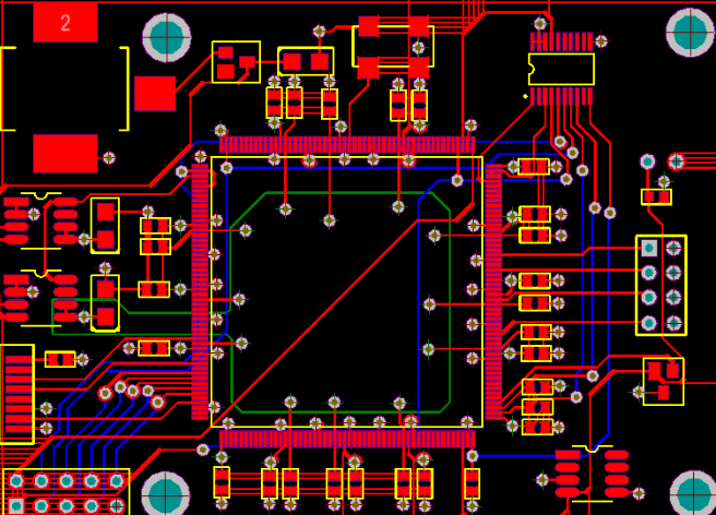
High-frequency PCBs operate on principles that prioritize signal integrity and minimal electromagnetic interference. At elevated frequencies, signals are prone to degradation due to factors like dielectric loss and skin effect. To counter this, these boards use low-loss dielectric materials with stable properties across a wide frequency range. The design also focuses on controlled impedance, ensuring consistent signal paths by carefully managing trace width and spacing.
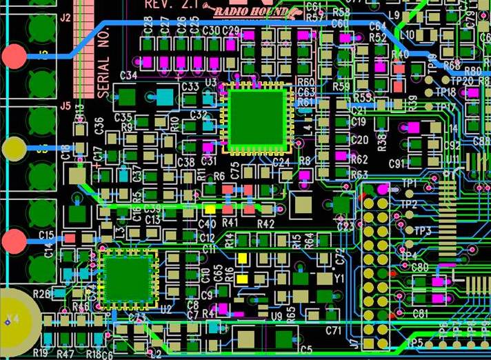
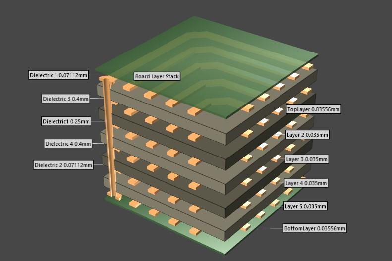
Grounding plays a crucial role in reducing noise and crosstalk. A solid ground plane beneath signal traces helps in maintaining signal quality by providing a return path for currents. Additionally, via placement and layer stack-up are optimized to prevent signal reflections. Adhering to standards like IPC-6012E for rigid board performance ensures that these designs meet industry benchmarks for reliability under high-frequency conditions.
Engineers must also consider thermal management since high-frequency signals can generate heat in compact designs. Proper material selection, aligned with standards such as IPC-A-600K for board acceptability, aids in dissipating heat effectively. These technical aspects collectively ensure that high-frequency PCBs deliver consistent performance in demanding applications.
Applications in Communication Systems
Communication systems rely heavily on high-frequency PCBs to support the rapid data transfer rates demanded by modern networks. These boards are integral to technologies like 5G infrastructure, where they enable high-speed signal transmission with low latency. Base stations and antennas use high-frequency PCBs to process signals in the gigahertz range, ensuring seamless connectivity across devices.
In satellite communication, these PCBs facilitate the transmission and reception of signals over long distances. Their ability to handle high-frequency bands allows for reliable data exchange between ground stations and orbiting satellites. Engineers designing such systems prioritize impedance control and signal isolation, often referencing guidelines from IPC-6012E to meet performance specifications.
Wireless devices, including routers and IoT modules, also depend on high-frequency PCBs for efficient operation. These boards ensure minimal signal loss, enabling stable connections in crowded frequency spectrums. For electrical engineers, understanding the role of high-frequency PCBs in communication systems is key to developing robust, future-ready technologies that support global connectivity.
Applications in Radar Systems
Radar systems, critical to defense, aviation, and automotive industries, utilize high-frequency PCBs for precise signal processing. These systems operate in frequency bands that require boards capable of handling rapid pulses and maintaining signal clarity. High-frequency PCBs are used in radar antennas and transceivers to detect objects with high accuracy, even in challenging environments.
In military applications, radar systems rely on these PCBs to process signals for surveillance and targeting. The boards must withstand harsh conditions while ensuring minimal signal distortion, often adhering to strict performance criteria outlined in standards like IPC-A-600K. Automotive radar, used in advanced driver-assistance systems, also depends on high-frequency PCBs to enable features like collision avoidance and adaptive cruise control.
The design of radar PCBs focuses on minimizing noise and optimizing signal paths. Engineers often employ multilayer configurations to separate sensitive components, reducing interference. For those working on radar technologies, high-frequency PCBs are essential to achieving the reliability and precision required for safety and security applications.
Applications in Medical Equipment
Medical equipment increasingly incorporates high-frequency PCBs to support advanced diagnostic and treatment technologies. Devices like MRI machines and ultrasound systems rely on these boards to process high-frequency signals for accurate imaging. The ability to transmit data without loss ensures that medical professionals receive clear, real-time information for patient care.
In wearable health monitors, high-frequency PCBs enable compact designs with efficient signal handling. These devices track vital signs and transmit data wirelessly, requiring boards that maintain performance in small form factors. Engineers designing medical PCBs must ensure compliance with standards like ISO 9001:2015 for quality management, guaranteeing reliability in critical applications.
High-frequency PCBs also play a role in therapeutic equipment, such as radiofrequency ablation devices. These systems demand precise control over signal delivery, which the boards facilitate through optimized designs. For electrical engineers in the medical field, leveraging high-frequency PCBs is vital to advancing healthcare technologies that improve patient outcomes.
Best Practices for Designing High-Frequency PCBs
Designing high-frequency PCBs requires careful attention to material selection, layout, and testing. Engineers should choose dielectric materials with low loss tangent values to minimize signal attenuation. The layer stack-up must be planned to balance signal layers with ground planes, reducing electromagnetic interference.
Trace geometry is another critical factor. Maintaining uniform trace widths and avoiding sharp bends helps prevent signal reflections. Impedance matching, guided by standards like IPC-6012E, ensures consistent performance across the board. Engineers should also minimize the use of vias in high-frequency paths to avoid inductance effects.
Thermal considerations are equally important. High-frequency signals can cause localized heating, so incorporating thermal vias and heat sinks is advisable. Testing the design for signal integrity, using methods aligned with IPC-A-600K, validates performance before production. By following these practices, electrical engineers can create high-frequency PCBs that meet the demands of communication systems, radar systems, and medical equipment.
Conclusion
High-frequency printed circuit boards are pivotal in driving advancements across multiple industries. Their applications in communication systems enable the high-speed connectivity required for modern networks like 5G. In radar systems, they ensure precision and reliability for critical functions in defense and automotive safety. Medical equipment benefits from these boards through enhanced diagnostic and therapeutic capabilities. For electrical engineers, understanding the technical principles and design best practices of high-frequency PCBs is essential to meeting the performance demands of these fields. By adhering to established industry standards and focusing on signal integrity, engineers can harness the full potential of these specialized boards to innovate and solve complex challenges in electronic design.
FAQs
Q1: How do high-frequency PCBs enhance communication systems?
A1: High-frequency PCBs are crucial in communication systems as they support rapid signal transmission with minimal loss. They enable technologies like 5G by handling gigahertz frequencies in base stations and wireless devices. Their design ensures stable connectivity, making them indispensable for engineers working on modern network infrastructure.
Q2: Why are high-frequency PCBs important for radar systems?
A2: Radar systems depend on high-frequency PCBs for accurate signal processing in detection and tracking. These boards manage high-frequency pulses, ensuring clarity in military and automotive applications. Their reliability, guided by strict standards, is vital for safety and security, as understood by engineers in the field.
Q3: What role do high-frequency PCBs play in medical equipment?
A3: In medical equipment, high-frequency PCBs facilitate precise signal handling for imaging devices like MRI and ultrasound systems. They support compact designs in wearable monitors, ensuring accurate data transmission. Engineers prioritize their quality to meet healthcare demands for reliable diagnostic and therapeutic tools.
Q4: What design challenges do engineers face with high-frequency PCBs?
A4: Designing high-frequency PCBs involves challenges like maintaining signal integrity and minimizing interference. Engineers must address impedance control and thermal management while adhering to industry standards. Overcoming these issues ensures performance in applications like communication systems, radar systems, and medical equipment.
IPC-6012E — Qualification and Performance Specification for Rigid Printed Boards. IPC, 2020.
IPC-A-600K — Acceptability of Printed Boards. IPC, 2020.
ISO 9001:2015 — Quality Management Systems. ISO, 2015.