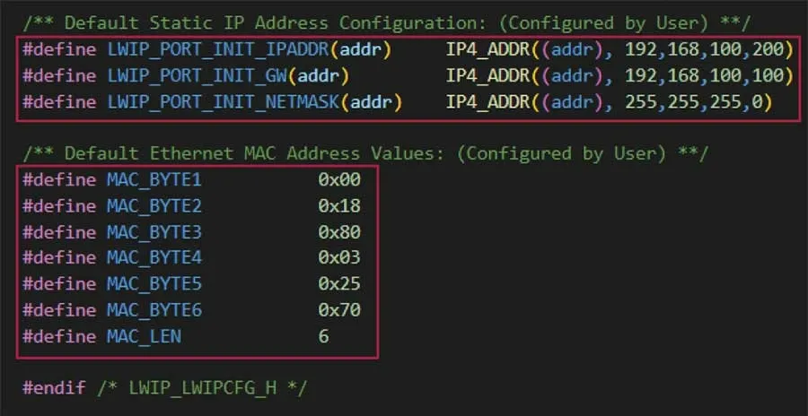
ALLPCB


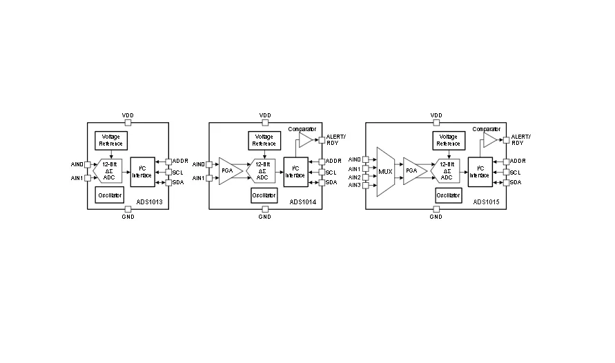
ADS1013, ADS1014 and ADS1015 (ADS101x) are high-precision, low-power, 12-bit, I2C-compatible analog-to-digital converters (ADC) from Texas Instruments. They are available in leadless X2QFN-10, SOT-10 and VSSOP-10 packages. ADS101x integrate a low-drift voltage reference and an oscillator. ADS1014 and ADS1015 also include a programmable gain amplifier (PGA) and a digital comparator. These features, together with a wide operating supply range, make the devices suitable for sensor measurement applications where power and board area are limited.
ADS101x can perform conversions at up to 3300 samples per second (SPS). The PGA supports input ranges from +/-256 mV to +/-6.144 V, enabling accurate measurement of both large and small signals. The ADS1015 includes an input multiplexer (MUX) for two differential or four single-ended inputs. The digital comparator in ADS1014 and ADS1015 can be used for under-voltage and over-voltage detection.
Features
- Ultra-compact packages:
- X2QFN: 1.5 mm x 2.0 mm x 0.4 mm
- SOT: 2.9 mm x 2.8 mm x 0.6 mm
- Noise-free resolution: 12-bit
- Wide supply range: 2.0 V to 5.5 V
- Low current consumption: 150 uA (continuous conversion mode)
- Programmable data rate: 128 SPS to 3.3kSPS
- Single-cycle settling
- Internal low-drift voltage reference
- Internal oscillator
- I2C interface: four pin-selectable addresses
- Operating temperature range: -40 C to +125 C
- Device family:
- ADS1013: 1 single-ended (SE) or differential (DE) input
- ADS1014: 1 single-ended or differential input, with comparator and PGA
- ADS1015: 4 single-ended or 2 differential inputs, with comparator and PGA
1. Product overview
ADS1013/ADS1014/ADS1015 are a series of high-precision, low-power ADCs from Texas Instruments. Key advantages include small size, multiple input configurations and flexible features. Typical applications include portable instruments, battery voltage/current monitoring, temperature measurement systems, consumer electronics and industrial automation. Devices operate from -40 C to +125 C and are available in X2QFN (1.5 mm x 2.0 mm), SOT (2.9 mm x 2.8 mm) and VSSOP (3 mm x 4.9 mm) packages. Single-supply operation is 2.0 V to 5.5 V. Integrated features include I2C, internal reference and oscillator, with programmable data rate and gain.
2. Key specifications and features
1. Core performance parameters
- Resolution and sample rate: 12-bit resolution with no missing codes; programmable data rate from 128 SPS to 3.3kSPS; single-cycle settling. Integral nonlinearity (INL) up to 0.5 LSB; typical offset error 0 LSB; typical gain error 0.05%.
- Dynamic and signal performance: ADS1014/ADS1015 include a programmable gain amplifier (PGA) with full-scale ranges (FSR) of +/-0.256 V to +/-6.144 V (six gain settings). ADS1013 has a fixed FSR of +/-2.048 V. Input impedance varies with FSR; common-mode input impedance up to 10 MOhm, differential input impedance up to 22 MOhm.
- Power and timing: Continuous conversion mode typical current 150 uA; power-down mode 0.5 uA. Supports I2C standard mode (100 kHz), fast mode (400 kHz) and high-speed mode (3.4 MHz).
2. Core features
- Inputs and signal handling: ADS1013 supports one differential or single-ended input. ADS1014 supports one differential or single-ended input. ADS1015 supports two differential or four single-ended inputs via an internal MUX. Output codes use two's complement format (-2048 to +2047) left-justified in a 16-bit register.
- Operating modes: Supports continuous and single-shot conversion modes. In single-shot mode the device powers down after each conversion to reduce idle power. Supports I2C general call reset to restore default configuration.
- Extended functions (ADS1014/ADS1015): Built-in digital comparator supports traditional and window comparator modes with configurable thresholds and trigger behavior. The ALERT/RDY pin can act as the comparator output or conversion-ready indicator, and supports latching and polarity configuration.
- Addressing and multi-device operation: ADDR pin selects one of four I2C addresses (0b1001000 to 0b1001011). Up to four devices can share the same I2C bus for multi-sensor systems.
3. Packaging and pins
1. Package information
- X2QFN (RUG): 10 pins, size 1.5 mm x 2.0 mm x 0.4 mm, reel packaging (3000 pcs/reel), MSL level 1 (260 C reflow, unlimited floor life).
- SOT (DYN): 10 pins, size 2.9 mm x 2.8 mm x 0.6 mm, reel packaging (3000 pcs/reel), MSL level 1.
- VSSOP (DGS): 10 pins, size 3 mm x 4.9 mm, available in 250-piece small reels and 2500-piece large reels, MSL level 2 (260 C reflow, 1 year floor life).
2. Key pin functions
- Power and ground: VDD (supply voltage, 2.0 V to 5.5 V) and GND. Place a 0.1 uF decoupling capacitor close to VDD to reduce supply noise.
- Signal inputs: AIN0 to AIN3 are analog input pins. ADS1013/ADS1014 use AIN0/AIN1 only. ADS1015 supports 4 input combinations.
- Communication and control: SCL (I2C clock input) and SDA (I2C data input/output) require 1 kOhm to 10 kOhm pull-up resistors. ADDR selects the I2C address. ALERT/RDY is the comparator output/conversion-ready pin (ADS1014/ADS1015 only).
4. Applications and design guidance
1. Typical applications
- Battery management: Monitor battery voltage and current for portable devices with low-power requirements.
- Temperature measurement: Use with thermistors, thermocouples and other temperature sensors for high-accuracy acquisition.
- Industrial control: Analog signal conversion in factory automation, supporting parallel multi-sensor acquisition (ADS1015).
2. Design resources
- Reference and supply: Internal low-drift voltage reference eliminates the need for an external reference. Use a clean, stable power supply and place decoupling capacitors close to VDD to avoid supply ripple affecting accuracy.
- Configuration notes: Configure operating mode, data rate, PGA gain and comparator parameters via four registers (conversion register, configuration register, high/low threshold registers). Single-shot and continuous modes are selectable through I2C register read/write operations.
- Layout guidelines: Separate analog and digital routing. Keep analog input pins away from noisy digital circuits. Match differential input trace lengths to minimize interference. Use solid ground planes to optimize return paths.
5. Reliability and ordering information
- Reliability: ESD protection meets JEDEC standards: human body model (HBM) +/-2000 V, charged device model (CDM) +/-500 V. Wide temperature range supports harsh environments.
- Orderable variants: ADS1013 (base version without PGA or comparator), ADS1014 (single-channel input with PGA and comparator), ADS1015 (multi-input with PGA and comparator). Each model is available in three package options. Package-specific part numbers identify package type (for example ADS1013IDGSR corresponds to the VSSOP package).