 ALLPCB


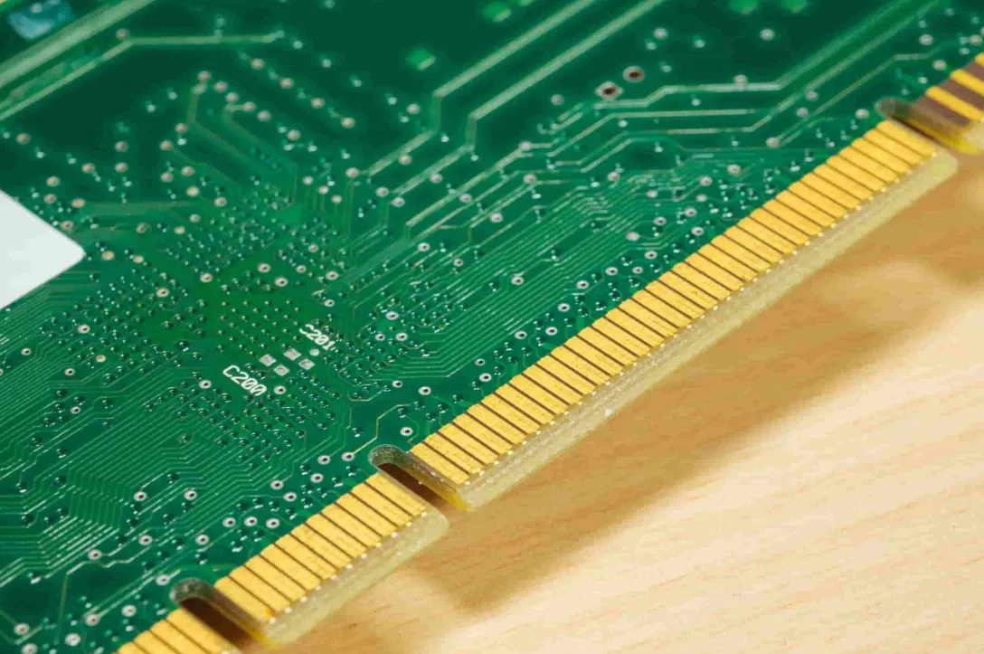
When it comes to designing printed circuit boards (PCBs) for high-reliability connections, selecting the right materials for gold fingers—also known as edge connectors—is critical. Gold fingers are the gold-plated pads on the edge of a PCB that facilitate connections between boards or sockets. The material composition for gold fingers directly impacts their durability, conductivity, and wear resistance. So, what are the best PCB gold finger plating materials? In short, hard gold plating, often alloyed with cobalt or nickel, is the go-to choice for most applications due to its superior wear resistance and conductivity. In this comprehensive guide, we’ll explore the nuances of hard gold plating, gold-cobalt alloy, gold-nickel alloy, and other factors related to gold finger wear resistance to help you make an informed decision for your specific application.
What Are PCB Gold Fingers and Why Do They Matter?
PCB gold fingers are the gold-plated connectors located on the edges of a circuit board. They serve as the interface for connecting a PCB to another board, socket, or device, commonly seen in applications like computer memory modules, graphics cards, and PCIe cards. These connectors are subjected to repeated insertion and removal, which makes their material composition and plating process vital for long-term performance.
The primary reason gold is used for these connectors is its excellent conductivity and resistance to corrosion. Unlike other metals that may tarnish or oxidize over time, gold maintains a stable connection even in harsh environments. However, pure gold is soft and prone to wear, which is why alloys and specific plating techniques are employed to enhance durability. Understanding the material composition for gold fingers can mean the difference between a reliable product and one that fails prematurely due to wear or poor connectivity.
The Basics of PCB Gold Finger Plating Materials
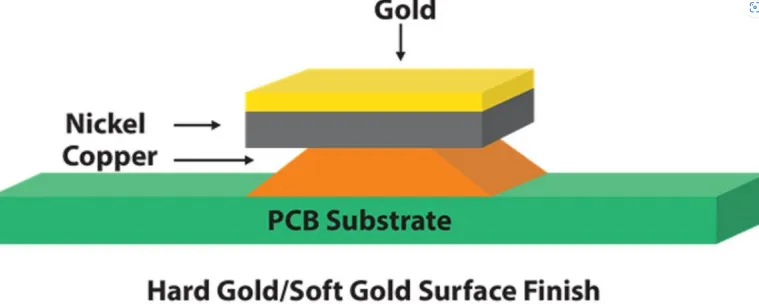
The process of plating gold fingers involves depositing a thin layer of gold over a base material, typically copper, with an intermediate layer of nickel. The choice of gold type and alloy plays a significant role in determining the connector’s performance. Let’s break down the key aspects of PCB gold finger plating materials.
Hard Gold Plating: The Industry Standard
Hard gold plating is the most common choice for gold fingers due to its enhanced durability. Unlike soft gold, which is pure and more prone to scratching, hard gold is alloyed with small amounts of other metals to improve its wear resistance. This type of plating can withstand thousands of insertion cycles—often up to 1,000 or more—without significant degradation, making it ideal for applications requiring frequent connections.
The thickness of hard gold plating typically ranges from 0.75 to 1.25 microns (30 to 50 microinches), depending on the application’s demands. Thicker layers provide better durability but increase costs. For high-reliability applications, such as military or aerospace equipment, thicker plating is often specified to ensure longevity under extreme conditions.
Intermediate Nickel Layer: A Foundation for Durability
Before gold is applied, a nickel layer—usually 2 to 6 microns thick—is plated onto the copper base. This nickel barrier prevents diffusion between copper and gold, which could otherwise lead to corrosion or reduced conductivity over time. Nickel also adds mechanical strength, supporting the gold layer during repeated use. Without this intermediate layer, the gold plating would wear off much faster, compromising the connector’s performance.
Exploring Gold Alloys for Enhanced Performance
While pure gold offers unmatched conductivity, its softness limits its use in high-wear applications. To address this, manufacturers often use gold alloys by combining gold with other metals like cobalt or nickel. These alloys strike a balance between conductivity and durability, ensuring that gold fingers can handle mechanical stress without sacrificing electrical performance. Let’s dive into the two most common options: gold-cobalt alloy and gold-nickel alloy.
Gold-Cobalt Alloy: Superior Wear Resistance
Gold-cobalt alloy is a popular choice for hard gold plating due to its excellent gold finger wear resistance. The addition of cobalt—typically around 0.1% to 0.3% by weight—hardens the gold, making it more resistant to abrasion and mechanical friction. This alloy is often used in applications where connectors are inserted and removed frequently, such as in consumer electronics and computer hardware.
One key advantage of gold-cobalt alloy is its ability to maintain a low contact resistance, often below 10 milliohms, even after thousands of cycles. This ensures a stable electrical connection over the product’s lifespan. Additionally, cobalt enhances the gold’s resistance to environmental factors like humidity and temperature fluctuations, making it suitable for demanding environments.
Gold-Nickel Alloy: Balancing Cost and Performance
Gold-nickel alloy is another common option for hard gold plating, offering a cost-effective alternative to gold-cobalt. The nickel content—usually less than 0.5%—provides similar hardening effects, improving the gold finger wear resistance compared to pure gold. While it may not match the durability of gold-cobalt alloy in extremely high-wear scenarios, it performs well in moderate-use applications and is often chosen for budget-conscious projects.
However, gold-nickel alloy can be slightly less resistant to corrosion in harsh environments compared to gold-cobalt. For applications exposed to high humidity or salty air, additional protective measures or a different alloy may be necessary to prevent long-term degradation.
Related Reading: Gold Fingers in PCBs: Applications and Manufacturing Standards
Factors Influencing Material Composition for Gold Fingers
Choosing the right material composition for gold fingers isn’t a one-size-fits-all decision. Several factors must be considered to ensure the selected alloy and plating thickness align with the application’s needs. Here are the key considerations:
Frequency of Use and Wear Resistance Needs
The number of insertion and removal cycles a connector will endure is a primary factor in material selection. For high-frequency use—such as in test equipment or modular systems—hard gold plating with a gold-cobalt alloy is often recommended. These materials can handle over 1,000 cycles without significant wear, maintaining signal integrity with impedance values typically below 50 ohms for controlled traces.
For low-frequency connections, where the PCB is inserted only a few times during its lifespan, a thinner layer of hard gold or even a gold-nickel alloy may suffice. This can help reduce manufacturing costs without compromising performance.
Environmental Conditions
The operating environment plays a significant role in material choice. Gold fingers in devices exposed to high humidity, temperature extremes, or corrosive gases require alloys with enhanced resistance to oxidation and tarnishing. Gold-cobalt alloys, combined with a robust nickel underlayer, are often the best choice for such conditions, as they provide a stable connection even after prolonged exposure.
Signal Integrity and Conductivity Requirements
In high-speed applications like PCIe cards, signal integrity is paramount. Gold fingers must maintain low contact resistance and minimize impedance mismatch, often targeting values around 85 to 100 ohms for differential pairs. Hard gold plating, regardless of the alloy, ensures excellent conductivity—second only to copper and silver—while the nickel layer prevents interference from the copper base. Choosing the right plating thickness and alloy ensures that signal speeds, often exceeding 5 Gbps in modern designs, are not compromised.
Related Reading: The Ultimate Guide to PCB Gold Finger Thickness: Balancing Cost and Performance
Cost Constraints
While gold offers unmatched performance, it’s also expensive. Thicker plating and premium alloys like gold-cobalt increase production costs. For projects with tight budgets, opting for a thinner hard gold layer or a gold-nickel alloy can provide a good balance between cost and reliability. It’s important to weigh the long-term benefits of durability against upfront expenses to make a cost-effective decision.
Best Practices for Designing PCB Gold Fingers
Beyond material selection, the design of gold fingers themselves can significantly impact their performance. Here are some best practices to ensure optimal results:
- Avoid Nearby Components: Keep surface-mount components, plated holes, and solder pads at least 1 mm away from gold fingers to prevent interference during insertion or plating.
- Copper Removal: Remove copper from inner layers beneath gold fingers to avoid exposure during beveling. A copper removal width of at least 3 mm is recommended to reduce impedance mismatch and enhance electrostatic discharge (ESD) protection.
- Length Limitations: Limit gold finger length to 40 mm or less to maintain structural integrity and consistent plating quality.
- Soldermask and Silkscreen: Avoid applying soldermask or silkscreen near gold fingers to prevent contamination or uneven plating.
Following these guidelines during the design phase ensures that the chosen PCB gold finger plating materials perform as expected, maximizing both durability and connectivity.

How to Choose the Right Alloy for Your Application
Selecting the best material composition for gold fingers requires a clear understanding of your project’s specific needs. Here’s a step-by-step approach to guide your decision:
- Assess Usage Frequency: Determine how often the connector will be used. High-frequency applications (over 500 cycles) benefit from gold-cobalt alloy with thicker hard gold plating.
- Evaluate Environmental Factors: Consider the operating conditions. Harsh environments call for alloys with superior corrosion resistance, such as gold-cobalt.
- Define Performance Requirements: Identify signal speed and impedance needs. High-speed designs prioritize low contact resistance and consistent plating thickness.
- Balance Cost and Quality: If budget is a concern, explore gold-nickel alloy or thinner plating for less demanding applications.
By carefully analyzing these factors, you can select a material and alloy that meets both technical and financial requirements, ensuring reliable performance over the product’s lifecycle.
Conclusion: Making an Informed Choice for PCB Gold Fingers
PCB gold fingers are a small but critical component of many electronic devices, and their material composition directly affects performance, durability, and cost. Hard gold plating, enhanced by alloys like gold-cobalt or gold-nickel, offers the wear resistance and conductivity needed for reliable connections. Gold-cobalt alloy excels in high-wear and harsh environments, while gold-nickel alloy provides a cost-effective alternative for moderate use. By considering factors like usage frequency, environmental conditions, signal requirements, and budget, you can choose the right PCB gold finger plating materials for your application.
At ALLPCB, we understand the importance of precision in every aspect of PCB manufacturing, from material selection to design optimization. Whether you’re working on a high-speed data card or a rugged industrial device, selecting the appropriate alloy and plating thickness for your gold fingers ensures long-lasting, high-quality connections. With the insights provided in this guide, you’re well-equipped to make an informed decision that balances performance and practicality for your next project.


