 ALLPCB


In the world of printed circuit board (PCB) design and manufacturing, precision is everything—especially when dealing with sensitive components. One critical technique that ensures precision and protects delicate parts during the production process is V-scoring. But what exactly is V-scoring, and why is it so important for minimizing stress and preventing component damage? In this comprehensive guide, we’ll dive deep into how V-scoring addresses design constraints and safeguards sensitive components, helping engineers and designers achieve reliable and high-quality results.
If you’re looking for a quick answer, V-scoring is a method used in PCB manufacturing to create V-shaped grooves on a panel, making it easier to separate individual boards without causing excessive stress or damage to sensitive components. Now, let’s explore this topic in detail, covering its benefits, challenges, and best practices for optimal design.
What Is V-Scoring and Why Does It Matter for PCBs?
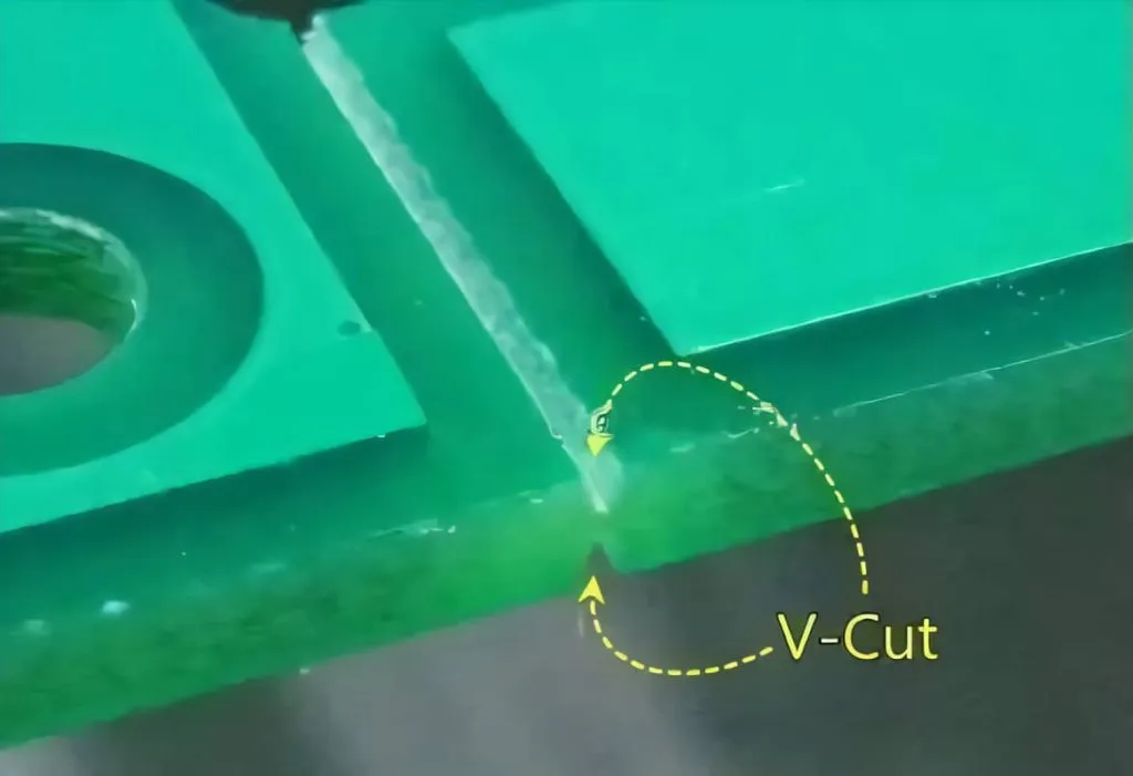
V-scoring, also known as V-grooving, is a manufacturing technique used to pre-cut grooves into a PCB panel. These grooves, shaped like a “V,” allow for clean and controlled separation of individual boards from a larger panel after assembly. This method is widely used in high-volume production because it streamlines the depaneling process and reduces mechanical stress on the board and its components.
For PCBs with sensitive components—such as microcontrollers, sensors, or fine-pitch ICs—V-scoring is especially critical. During depaneling, improper separation methods can cause vibrations, bending, or twisting, which may crack solder joints, dislodge components, or damage the board itself. V-scoring minimizes these risks by providing a predetermined breaking point that requires minimal force to separate.
The Importance of Protecting Sensitive Components
Sensitive components are often the heart of modern electronic devices. These parts, which can include surface-mount devices (SMDs), ball grid arrays (BGAs), or micro-electromechanical systems (MEMS), are highly susceptible to mechanical stress. For instance, a BGA package with hundreds of tiny solder balls can fail if even a small amount of stress disrupts the connections during depaneling.
Statistics highlight the stakes: studies in the electronics industry suggest that up to 15% of PCB failures during manufacturing can be attributed to mechanical stress during handling or separation. When dealing with high-value or delicate components, such failures can lead to significant costs and delays. V-scoring helps mitigate these risks by ensuring a controlled separation process that reduces V-score stress on the board.
Additionally, sensitive components often have strict design constraints. They may require precise placement near the board’s edge or specific thermal and electrical tolerances. Without a careful depaneling method like V-scoring, meeting these constraints becomes nearly impossible.
How V-Scoring Reduces Stress and Component Damage
The primary advantage of V-scoring is its ability to minimize mechanical stress during the depaneling process. Here’s how it works:
- Controlled Breakage: The V-shaped groove acts as a stress-relief point, guiding the break along a specific line. This reduces the force needed to separate boards, lowering the risk of unintended cracks or bending.
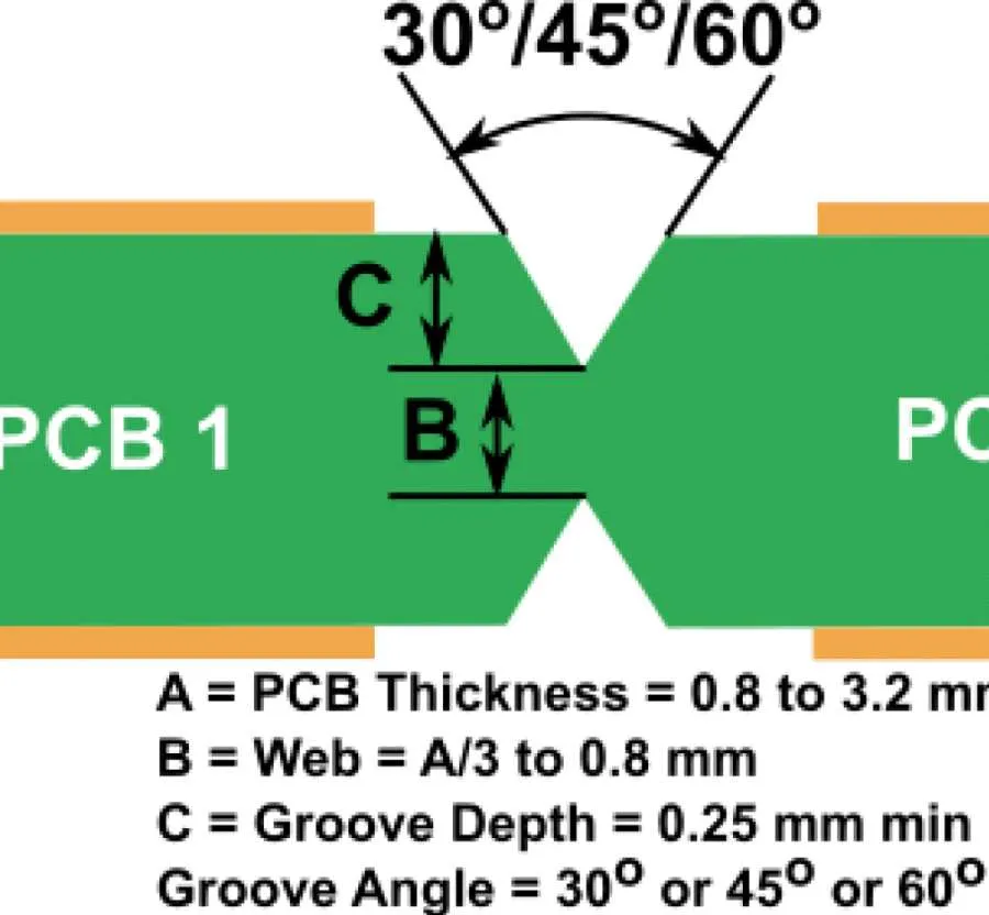
- Uniform Depth: V-scoring machines are designed to cut grooves with precise depths, typically leaving a residual thickness of 0.3 to 0.6 mm, depending on the board material and thickness (common FR-4 boards are often 1.6 mm thick). This uniformity ensures consistent results across an entire panel.
- Minimal Vibration: Unlike manual breaking or routing methods, V-scoring creates less vibration, which is crucial for protecting sensitive components from micro-cracks or solder joint failures.
By reducing V-score stress, this technique directly addresses the risk of component damage. For example, a PCB with a high-density interconnect (HDI) design might include components with pitches as small as 0.4 mm. Excessive stress during depaneling could misalign or break these connections, leading to costly rework. V-scoring ensures that such risks are kept to a minimum.
Design Constraints and Challenges with V-Scoring
While V-scoring offers significant benefits, it also comes with specific design constraints that engineers must consider to avoid issues. Understanding these limitations is key to preventing component damage and ensuring a successful manufacturing process.
1. Component Placement Near Score Lines
One of the most critical design constraints is the placement of sensitive components near the V-score line. If components are too close to the groove, the stress of breaking—even with a controlled method—can still affect them. As a general rule, manufacturers recommend a minimum clearance of 5 mm between the score line and any component. For particularly delicate parts, this distance may need to be increased to 8-10 mm.
2. Board Thickness and Material
The thickness and material of the PCB also influence the effectiveness of V-scoring. Standard FR-4 boards with thicknesses between 0.8 mm and 2.0 mm are ideal for V-scoring. However, thinner boards (below 0.6 mm) may be too fragile, while thicker boards (above 2.4 mm) may require deeper grooves, increasing the risk of stress concentration. Additionally, flexible or rigid-flex PCBs may not be suitable for V-scoring due to their unique material properties.
3. Score Line Alignment
V-scoring requires precise alignment of the grooves on both the top and bottom sides of the board. Misalignment by even 0.1 mm can lead to uneven breaking, causing stress or cracks that could propagate to sensitive components. Modern scoring machines typically achieve tolerances of ±0.05 mm, but designers must still account for potential variations during manufacturing.
4. Panel Size and Layout
Larger panels with multiple boards can introduce additional design constraints. For instance, if a panel exceeds 300 mm in length, the risk of bowing or warping during scoring increases, potentially leading to uneven stress distribution. Designers must balance panel size with the need for efficient production while ensuring that sensitive components are protected.

Best Practices for V-Scoring in PCB Design
To maximize the benefits of V-scoring and protect sensitive components, engineers should follow these best practices during the design and manufacturing stages:
- Optimize Component Layout: Keep sensitive components at least 5-10 mm away from score lines. Use design software to simulate stress distribution and identify potential weak points near the edges.
- Specify Scoring Parameters: Clearly define the depth and angle of the V-groove in your design files. Common angles are 30° or 45°, with a residual thickness of about 1/3 of the board’s total thickness (e.g., 0.5 mm for a 1.6 mm board).
- Choose Compatible Materials: Stick to standard PCB materials like FR-4 for V-scoring. If using alternative materials, consult with your manufacturer to ensure compatibility.
- Test Prototypes: Before full-scale production, test a small batch of panels to verify that the scoring process does not introduce stress or damage to components. Use tools like X-ray inspection to check for micro-cracks in solder joints.
- Collaborate with Manufacturers: Work closely with your manufacturing partner to ensure that their equipment and processes align with your design requirements. Provide detailed documentation, including scoring guidelines and component datasheets.
By adhering to these practices, you can significantly reduce the risk of component damage and ensure that V-scoring works effectively for your project.
Comparing V-Scoring to Other Depaneling Methods
To fully appreciate the value of V-scoring, it’s helpful to compare it to other common depaneling methods. Each approach has its strengths and weaknesses, especially when it comes to protecting sensitive components.
- Routing: This method uses a CNC router to cut through the panel. While it offers high precision, it generates significant dust and vibration, which can harm delicate components. Routing is also slower and more expensive than V-scoring for large-scale production.
- Breakaway Tabs: Also known as mousebites, these are small perforated tabs that hold boards together. They are simple to implement but often require manual separation, which can introduce uneven stress and increase the risk of component damage.
- Laser Cutting: Laser depaneling provides extreme precision and minimal mechanical stress, making it ideal for sensitive components. However, it is costly and not suitable for high-volume production due to slower processing times.
V-scoring strikes a balance between cost, efficiency, and stress reduction, making it a preferred choice for many applications involving sensitive components. Its ability to handle high-volume production while minimizing V-score stress sets it apart from other methods.
Real-World Applications of V-Scoring for Sensitive Components
V-scoring is widely used across various industries where sensitive components are common. Here are a few examples:
- Automotive Electronics: Modern vehicles rely on PCBs with sensors and control units that must withstand harsh conditions. V-scoring ensures these components are not damaged during manufacturing, maintaining reliability.
- Medical Devices: Devices like pacemakers or diagnostic tools often use tiny, high-precision components. V-scoring helps protect these parts, ensuring patient safety and device accuracy.
- Consumer Electronics: Smartphones and wearables pack sensitive components into compact designs. V-scoring allows manufacturers to produce these devices efficiently without compromising quality.
In each of these cases, V-scoring addresses design constraints and reduces the risk of component damage, proving its value in high-stakes applications.
Conclusion: Precision and Protection with V-Scoring
When precision matters, V-scoring stands out as an essential technique for PCB manufacturing, especially for designs with sensitive components. By reducing V-score stress and minimizing the risk of component damage, this method helps engineers meet strict design constraints while maintaining efficiency in production. Whether you’re working on automotive systems, medical devices, or consumer electronics, incorporating V-scoring into your design process can make a significant difference in quality and reliability.
At ALLPCB, we understand the importance of precision in every step of PCB manufacturing. Our advanced V-scoring capabilities ensure that your sensitive components are protected, delivering panels that meet your exact specifications. By following best practices and collaborating closely with your manufacturing partner, you can achieve outstanding results for even the most complex projects.


