 ALLPCB


In the world of electronics, innovation never stops. One of the most exciting advancements is the development of transparent PCBs, also known as clear circuit boards. These see-through electronics are not just visually stunning but also open up new possibilities for unique PCB projects and display PCB applications. At ALLPCB, we’re thrilled to dive into this cutting-edge technology, exploring how glass substrates are used to create transparent PCBs and why they’re shaping the future of electronics.
In this blog, we’ll cover everything you need to know about transparent PCBs, from their materials and manufacturing to their applications and benefits. Whether you’re an engineer, designer, or tech enthusiast, this guide will help you understand the potential of see-through electronics and inspire your next project.
What Are Transparent PCBs?
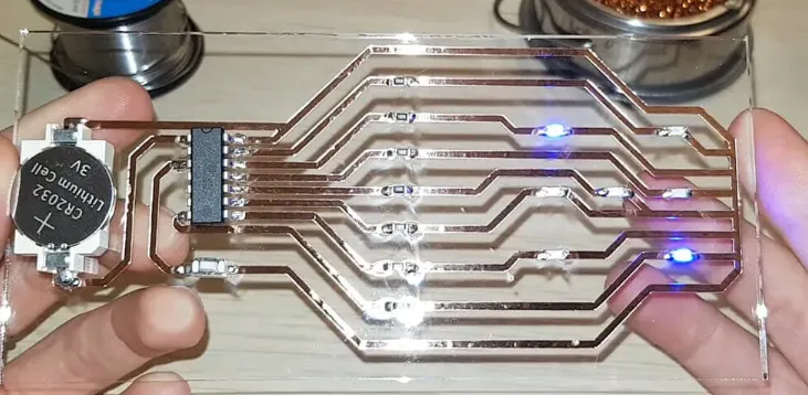
A transparent PCB is a type of printed circuit board that uses a clear substrate material instead of the traditional opaque options like FR-4. This allows the board to be see-through while still supporting the necessary electrical components and conductive traces. The result is a functional circuit board with a unique, futuristic aesthetic that’s perfect for display PCB designs and innovative electronics.
Unlike standard PCBs, which prioritize durability and cost over appearance, transparent PCBs focus on both functionality and visual appeal. They’re often made from materials like glass or specialized polymers, which we’ll explore in more detail below. These materials enable applications where transparency is key, such as in optical devices or consumer electronics with exposed internals.
Materials Behind Clear Circuit Boards
The core of any transparent PCB lies in its substrate material. While traditional PCBs rely on fiberglass or epoxy-based materials, clear circuit boards use alternatives that allow light to pass through. Here are the primary materials used in creating see-through electronics:
- Glass Substrates: Glass is a popular choice for transparent PCBs due to its excellent optical clarity and thermal stability. It can withstand high temperatures, making it suitable for demanding applications. However, glass is brittle and requires careful handling during manufacturing and use.
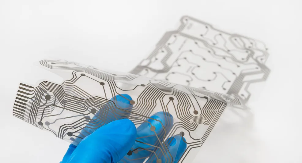
- Polymer Films: Flexible transparent PCBs often use polymer films like polyethylene terephthalate (PET) or polyimide (PI). These materials are lightweight and bendable, ideal for foldable devices or curved displays, though they may not match glass in terms of heat resistance.
- Transparent Conductive Materials: For the conductive traces, materials like indium tin oxide (ITO) or silver nanowires are used. These provide electrical conductivity while maintaining transparency, though they can be more expensive than traditional copper.
How Are Transparent PCBs Manufactured?
Creating a clear circuit board involves specialized processes to ensure both transparency and functionality. While the core principles of PCB manufacturing remain, such as etching and layering, the materials and techniques differ. Here’s a simplified overview of the process:
- Substrate Preparation: The chosen transparent material, like glass, is cleaned and prepared to ensure a smooth surface for trace deposition. Any imperfections can affect both clarity and electrical performance.
- Conductive Layer Application: A thin layer of transparent conductive material, such as ITO, is applied to the substrate. This layer forms the pathways for electrical signals.
- Patterning: Using photolithography or laser etching, the conductive material is patterned into the desired circuit design. Precision is critical to avoid damaging the delicate substrate.
- Component Mounting: Electronic components are mounted onto the board using techniques like surface-mount technology (SMT). Special care is taken to ensure alignment and stability, especially on rigid glass substrates.
- Testing: The finished transparent PCB undergoes rigorous testing for electrical performance and optical clarity. Signal integrity is often checked, with impedance values typically ranging between 50 to 100 ohms for high-speed applications.
Manufacturing transparent PCBs requires advanced equipment and expertise due to the unique challenges posed by materials like glass. For instance, glass substrates have a dielectric constant of around 5.5 to 7.0, compared to FR-4’s 4.5, which can affect signal speeds in high-frequency designs.
Applications of See-Through Electronics
Transparent PCBs are not just about looks; they serve practical purposes in various industries. Their unique properties make them ideal for specific applications where traditional boards fall short. Here are some key areas where clear circuit boards shine:
1. Display Technology
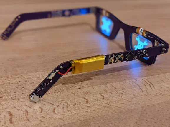
In display PCB designs, transparency is crucial. Transparent PCBs are used in LED screens, touch panels, and augmented reality (AR) devices where users need to see through the board. For example, in AR glasses, a clear circuit board allows for unobstructed vision while supporting the necessary electronics.
2. Optical Devices
Transparent PCBs play a vital role in optical applications like cameras and sensors. Their ability to minimize light scattering improves the efficiency of these devices. Signal speeds in optical systems often exceed 10 Gbps, and transparent materials help maintain performance by reducing interference.
3. Consumer Electronics
From smartphones with visible internals to smartwatches with sleek designs, see-through electronics are becoming a trend in consumer products. They offer a modern, high-tech aesthetic that appeals to customers looking for unique PCB projects.
4. Medical Equipment
In medical devices, transparent PCBs are used in diagnostic tools where clarity and precision are essential. Their compatibility with optical systems makes them suitable for imaging equipment, ensuring accurate results.
Benefits of Using Transparent PCBs
Why choose a transparent PCB over a traditional one? The advantages go beyond aesthetics and align with the needs of modern electronics. Here are the main benefits:
- Visual Appeal: Transparent PCBs offer a futuristic look that’s perfect for showcasing internal components in unique PCB projects. They’re often used in products where design is as important as function.
- Optical Efficiency: In applications like displays and sensors, clear circuit boards reduce light loss, improving performance. This is especially critical in devices where every photon counts.
- Flexibility in Design: With materials like polymer films, transparent PCBs can be flexible, allowing for innovative shapes and foldable devices. This opens up possibilities for compact and portable electronics.
- Thermal Stability: Glass-based transparent PCBs can handle high temperatures, with some substrates rated for up to 300°C, making them suitable for harsh environments.
Challenges of Transparent PCBs
While transparent PCBs offer incredible potential, they come with certain challenges that engineers must consider during design and production:
- Fragility: Glass substrates, while thermally stable, are prone to breaking under mechanical stress. This limits their use in applications requiring durability.
- Cost: Materials like ITO and high-quality glass are more expensive than standard PCB materials. Production costs can be 20-30% higher, depending on the complexity of the design.
- Manufacturing Complexity: Working with transparent materials requires specialized equipment and techniques, which can increase lead times and require skilled labor.
- Limited Conductivity: Transparent conductive materials often have higher resistance compared to copper, with resistivity values for ITO around 10^-4 ohm-cm, potentially affecting performance in high-power applications.
Tips for Designing Unique PCB Projects with Transparent Boards
If you’re inspired to create your own see-through electronics, here are some practical tips to ensure success in your unique PCB projects:
- Choose the Right Material: Decide between glass for rigidity and thermal resistance or polymer films for flexibility. Consider the environment your PCB will operate in.
- Optimize for Transparency: Minimize the use of opaque components or coatings that could block light. Use transparent soldermask or adhesives where possible.
- Test Signal Integrity: Due to the different dielectric properties of transparent materials, simulate and test your design for impedance matching and signal speeds. Aim for controlled impedance values, often around 50 ohms for digital signals.
- Work with Experts: Partner with a reliable manufacturing service to handle the complexities of transparent PCB production. At ALLPCB, we provide support for innovative designs, ensuring quality and precision.
- Focus on Aesthetics: Since transparency is a key feature, design your layout to highlight the internal traces and components as part of the visual appeal.
The Future of Transparent PCBs in Electronics
The demand for transparent PCBs is growing as industries push for more innovative and visually appealing electronics. With advancements in materials science, we’re seeing improvements in the durability and conductivity of clear circuit boards. For instance, research into graphene-based conductors promises to lower resistance while maintaining transparency, potentially reducing resistivity to below 10^-6 ohm-cm.
In the near future, transparent PCBs could become standard in wearable technology, smart home devices, and automotive displays. Their ability to blend seamlessly into designs while supporting high-speed signals (up to 25 Gbps in some prototypes) makes them a game-changer for next-generation electronics.
Why Choose ALLPCB for Your Transparent PCB Needs?
At ALLPCB, we’re committed to helping you bring your innovative ideas to life. Whether you’re working on display PCB designs or unique PCB projects with see-through electronics, we offer end-to-end support. Our advanced manufacturing capabilities ensure that your transparent PCBs meet the highest standards of quality and performance.
From material selection to final testing, we provide expertise at every step. Our team understands the nuances of working with glass and polymer substrates, ensuring precise trace deposition and reliable electrical performance. Partner with us to explore the possibilities of transparent PCBs and create electronics that stand out.
Conclusion
Transparent PCBs are revolutionizing the electronics industry, offering a perfect blend of functionality and aesthetics. Using glass and other clear materials, these see-through electronics are paving the way for innovative applications in display technology, optical devices, and consumer products. While challenges like cost and fragility exist, the benefits of optical efficiency and design flexibility make transparent PCBs a compelling choice for unique PCB projects.
As technology continues to evolve, clear circuit boards will play an even bigger role in shaping the future of electronics. At ALLPCB, we’re excited to be part of this journey, providing the tools and expertise you need to create cutting-edge designs. Start exploring the world of transparent PCBs today and see how they can transform your next project.


