 ALLPCB


In the world of high-power electronics, managing heat in complex designs like 14-layer PCBs is critical. If you're wondering how to handle 14-layer PCB thermal design or improve PCB heat dissipation, you've come to the right place. This blog dives deep into proven thermal management multilayer PCB strategies, focusing on techniques like thermal vias in PCBs and effective methods for cooling high-power PCBs. We'll break down practical solutions to keep your boards running efficiently and reliably under demanding conditions.
Why Thermal Management Matters for 14-Layer PCBs
High-power 14-layer PCBs are often used in advanced applications like telecommunications, industrial equipment, and aerospace systems. These multilayer boards pack a lot of components and power into a compact space, generating significant heat. Without proper thermal management multilayer PCB strategies, excessive heat can lead to component failure, reduced performance, and shorter product lifespans. Studies show that for every 10°C rise in temperature, the lifespan of electronic components can be halved. That’s why mastering PCB heat dissipation is non-negotiable for engineers working on high-density designs.
In this guide, we'll explore the unique challenges of 14-layer PCB thermal design and provide actionable techniques to ensure your boards stay cool and reliable.
Understanding the Challenges of Heat in High-Power 14-Layer PCBs
A 14-layer PCB is a complex structure with multiple signal, power, and ground planes stacked together. This high layer count allows for intricate routing and high-speed signal transmission, often exceeding 5 GHz in modern designs. However, it also creates unique thermal challenges:
- High Power Density: Components like power amplifiers and processors generate heat in a confined area, raising the risk of hotspots.
- Limited Airflow: With multiple layers, heat struggles to escape from internal layers, especially in compact enclosures.
- Material Constraints: The dielectric materials used in multilayer boards often have lower thermal conductivity, trapping heat.
Addressing these issues requires a combination of design techniques and material choices tailored for cooling high-power PCBs. Let’s dive into the most effective solutions.
Key Thermal Management Techniques for 14-Layer PCBs
1. Optimize Component Placement for Heat Distribution
Strategic component placement is the first step in 14-layer PCB thermal design. High-power components should be spaced out to avoid creating concentrated heat zones. Place heat-generating components like voltage regulators or high-speed processors near the edges of the board, where airflow is typically better. Additionally, ensure sensitive components, such as analog circuits, are positioned away from heat sources to maintain signal integrity.
For example, if a processor on your board dissipates 15W of power, placing it centrally on an internal layer could cause temperatures to spike above 85°C, the typical maximum for many components. Moving it closer to a board edge or near a heat sink can reduce this by 20-30%.
2. Use Thermal Vias for Efficient Heat Transfer
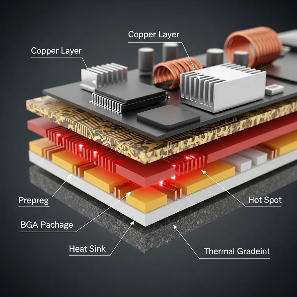
One of the most effective tools for PCB heat dissipation is the use of thermal vias in PCBs. These are small plated-through holes that transfer heat from one layer to another, often connecting hot components to a ground or power plane that acts as a heat spreader. In a 14-layer PCB, thermal vias are especially useful for moving heat from internal layers to outer layers, where it can dissipate more easily.
A typical thermal via array might include vias with a diameter of 0.3mm and a pitch of 1.2mm, placed directly under high-power components. Research suggests that adding thermal vias can reduce component junction temperatures by up to 15°C in high-power designs. However, avoid overusing vias, as they can interfere with signal routing and increase manufacturing costs.
3. Select High-Thermal-Conductivity Materials
The choice of materials plays a huge role in thermal management multilayer PCB designs. Standard FR-4 material has a thermal conductivity of about 0.3 W/m·K, which is insufficient for high-power applications. For 14-layer PCBs, consider using advanced laminates with higher thermal conductivity, such as those infused with ceramic fillers, which can reach up to 3 W/m·K.
Additionally, opt for thicker copper layers on power and ground planes. A 2 oz/ft2 copper layer can handle higher currents and dissipate heat more effectively than a standard 1 oz/ft2 layer, reducing temperature rises by as much as 10°C in critical areas.
4. Incorporate Heat Sinks and Thermal Pads
For cooling high-power PCBs, external solutions like heat sinks are often necessary. Attach heat sinks to high-power components to increase the surface area for heat dissipation. Ensure the heat sink is properly sized—a heat sink with a thermal resistance of 2°C/W can manage a 20W component effectively in most ambient conditions.
Thermal pads or interface materials between the component and heat sink are also critical. These materials, often with thermal conductivities of 1-5 W/m·K, fill air gaps and improve heat transfer. In a 14-layer PCB design, combining heat sinks with internal thermal vias creates a robust cooling pathway from inner layers to the external environment.
5. Design for Active Cooling Solutions
In extreme cases, passive cooling might not be enough for high-power 14-layer PCBs. Active cooling, such as fans or liquid cooling systems, can be integrated into the design. For instance, a small fan providing 10 CFM (cubic feet per minute) of airflow can lower board temperatures by 15-20°C compared to natural convection alone.
When designing for active cooling, ensure mounting holes or brackets for fans are included in the PCB layout. Also, position components to align with airflow paths, maximizing the cooling effect across the board.
6. Leverage Ground and Power Planes as Heat Spreaders
In a 14-layer PCB, you have multiple ground and power planes at your disposal. These copper planes can act as natural heat spreaders, distributing heat away from hotspots. Dedicate at least one or two internal layers as solid copper planes connected to thermal vias for maximum effect. A solid ground plane with 2 oz/ft2 copper can reduce thermal resistance by up to 30% compared to a fragmented plane.
Be mindful of signal integrity, though. Avoid placing high-speed traces near these planes if they carry significant heat, as thermal expansion can affect impedance, typically around 50 ohms for standard designs.
Advanced Strategies for PCB Heat Dissipation
Thermal Simulation and Modeling
Before finalizing your 14-layer PCB thermal design, use thermal simulation tools to predict heat distribution and identify potential issues. Software can model heat flow, showing areas where temperatures might exceed safe limits, such as 85°C for most ICs. By simulating a design with a 25W power source, you might find that adding just 10 thermal vias drops the peak temperature from 90°C to 75°C, a significant improvement.
Thermal modeling also helps optimize via placement and heat sink sizing, saving time and cost during prototyping.
Embedded Heat Pipes for Extreme Cases
For ultra-high-power applications, consider embedding heat pipes within the PCB structure. These are thin, hollow tubes filled with a working fluid that transfers heat rapidly through evaporation and condensation. While more common in specialized designs, heat pipes can reduce hotspot temperatures by up to 40% in multilayer boards. Note that this approach increases complexity and cost, so reserve it for critical projects.
Best Practices for Cooling High-Power PCBs
To wrap up, here are some best practices to ensure effective PCB heat dissipation in your 14-layer designs:
- Start thermal planning early in the design phase to avoid costly revisions.
- Combine multiple techniques, such as thermal vias, heat sinks, and material upgrades, for a comprehensive approach.
- Monitor ambient conditions—designs for industrial environments (often 40-60°C ambient) need more aggressive cooling than consumer products.
- Iterate designs based on thermal testing results, using tools like infrared cameras to spot heat issues post-assembly.
Conclusion
Managing heat in high-power 14-layer PCBs is a complex but essential task. By implementing the thermal management multilayer PCB techniques discussed—such as optimizing component placement, using thermal vias in PCBs, selecting the right materials, and incorporating heat sinks—you can significantly improve PCB heat dissipation and ensure reliability. Whether you're tackling 14-layer PCB thermal design for telecommunications or industrial systems, these strategies for cooling high-power PCBs will help you achieve optimal performance.
At ALLPCB, we understand the intricacies of multilayer PCB designs and are committed to supporting your projects with high-quality manufacturing solutions. Apply these thermal management tips to your next design and see the difference in performance and durability.


