ALLPCB


As smart home technology continues to evolve, the demand for advanced printed circuit boards (PCBs) is growing rapidly. What does the future hold for PCB design in smart home applications? In short, the future of smart home PCBs is shaped by trends like embedded components, 3D printed electronics, biodegradable materials, and cutting-edge PCB technology advancements. These innovations are paving the way for smaller, more efficient, and environmentally friendly devices that power everything from smart thermostats to connected lighting systems.
In this blog, we’ll dive deep into the key trends and innovations driving the future of PCB design for smart homes. From miniaturization to sustainability, we’ll explore how these advancements are transforming the industry and what they mean for engineers and designers. Let’s get started on this journey into the next generation of smart home technology.
Why Smart Home PCBs Are Evolving Rapidly
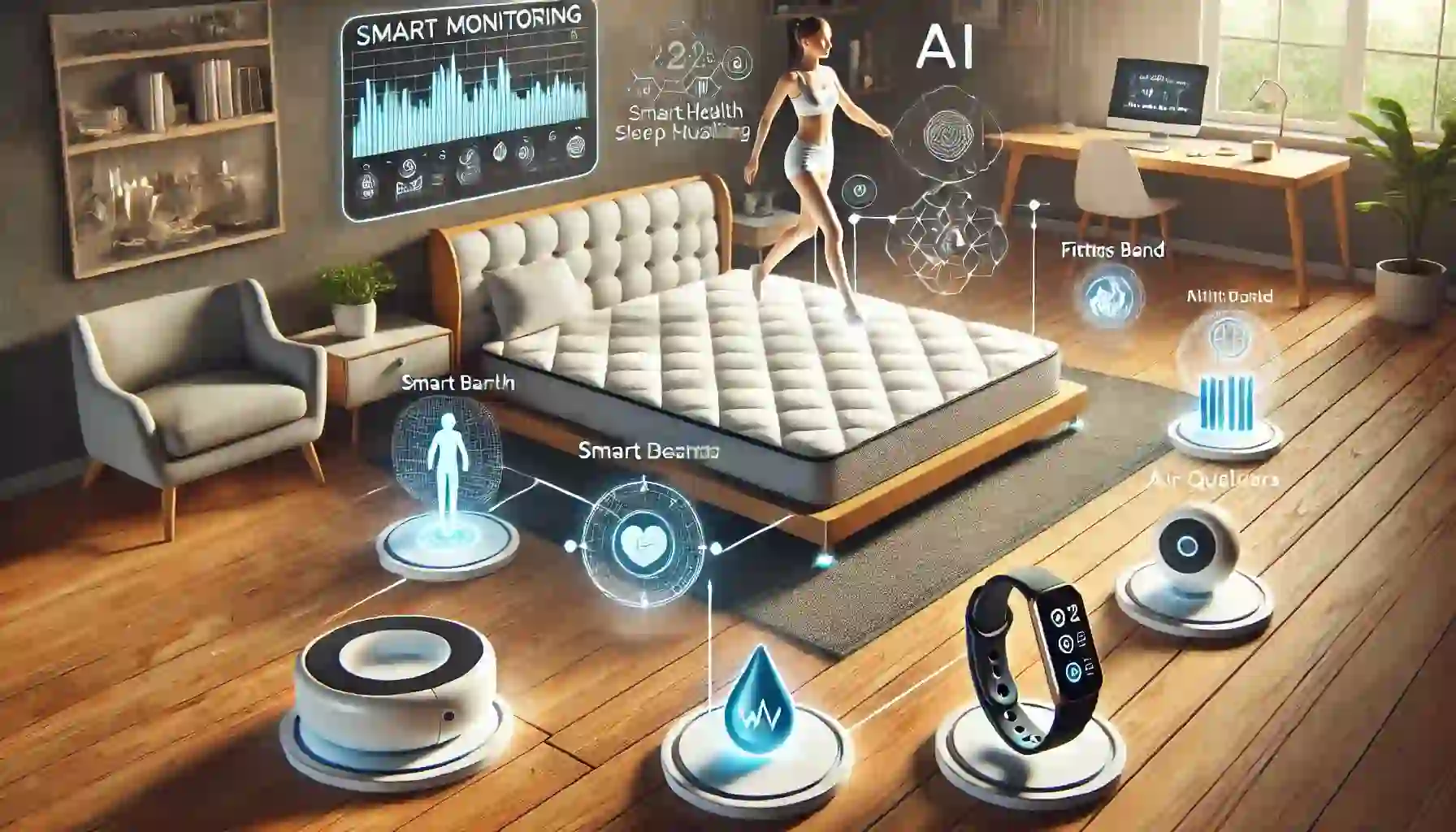
Smart home devices are becoming more complex, with a growing need for seamless connectivity, energy efficiency, and compact designs. PCBs, as the backbone of these devices, must adapt to meet these demands. The rise of the Internet of Things (IoT) means that every smart device—whether it’s a voice-activated speaker or a security camera—requires a PCB that can handle high-speed data transfer, low power consumption, and integration with multiple sensors.
According to industry estimates, the global smart home market is expected to reach over $150 billion by 2026, with millions of connected devices relying on innovative PCB solutions. This rapid growth pushes designers to adopt new materials, manufacturing techniques, and design approaches to stay ahead. Let’s explore the major trends shaping the future of PCB design for smart homes.
Trend 1: Miniaturization with Embedded Components
One of the most significant trends in future PCB design is miniaturization, driven by the integration of embedded components. Smart home devices are getting smaller, yet they need to pack more functionality into limited space. Embedding components like resistors, capacitors, and even microcontrollers directly into the PCB layers reduces the overall footprint and improves performance.
For instance, embedding a capacitor within the PCB can reduce parasitic inductance, leading to better signal integrity at high frequencies—often above 1 GHz, which is critical for Wi-Fi and Bluetooth connectivity in smart devices. This approach also cuts down on assembly costs and enhances reliability by minimizing the number of soldered connections.
Embedded components are particularly useful in smart home applications like wearable devices or compact IoT sensors, where space is at a premium. As this technology advances, we expect to see even smaller PCBs with higher component density, enabling sleeker and more discreet smart home products.
Trend 2: 3D Printed Electronics for Custom Smart Home Solutions
Another game-changer in PCB technology trends is the rise of 3D printed electronics. Traditional PCB manufacturing involves multiple steps, including etching and drilling, which can be time-consuming and limit design flexibility. 3D printing, on the other hand, allows for rapid prototyping and the creation of complex, custom geometries that are ideal for unique smart home applications.
With 3D printed electronics, conductive traces and insulating layers can be printed directly onto a substrate, or even onto non-flat surfaces, enabling PCBs to be integrated into curved or irregular shapes. Imagine a smart light switch with a PCB printed directly into its housing, reducing assembly steps and creating a more seamless design. This technology also supports the use of flexible materials, which can withstand bending and stretching—perfect for wearable smart home controllers.
While still in its early stages, 3D printed electronics are expected to lower production costs and reduce waste, making them a promising option for future PCB design. For engineers, this means faster iteration cycles and the ability to test innovative ideas without the constraints of traditional manufacturing.
Trend 3: Biodegradable PCBs for Sustainable Smart Homes
Sustainability is a growing concern in electronics, and biodegradable PCBs are emerging as a key innovation for environmentally conscious smart home designs. Traditional PCBs are made from materials like fiberglass and epoxy, which are difficult to recycle and contribute to electronic waste. With millions of smart home devices being produced each year, the environmental impact is significant.
Biodegradable PCBs use alternative substrates, such as cellulose-based materials or bio-resins, that can break down naturally over time. These materials are still in development, but early research shows promising results. For example, some biodegradable substrates can maintain thermal stability up to 200°C, making them suitable for low-power smart home devices like temperature sensors or smart plugs.
While performance and durability challenges remain, the push for green technology is driving investment in biodegradable PCBs. For smart home manufacturers, adopting these materials can improve brand reputation and meet stricter environmental regulations. As this trend grows, we anticipate a future where sustainable PCB design becomes the norm rather than the exception.
Trend 4: High-Speed Connectivity with Advanced Materials
Smart home devices rely heavily on fast and reliable connectivity, whether it’s for real-time data streaming or low-latency communication between devices. PCB technology trends are addressing this need through the use of advanced materials that support high-speed signals, especially for 5G and Wi-Fi 6 applications.
Materials like low-loss laminates and high-frequency substrates are becoming more common in PCB design. These materials minimize signal loss at frequencies above 5 GHz, ensuring that smart home devices like security cameras or streaming hubs maintain consistent performance. For example, a low-loss material with a dielectric constant (Dk) of 3.0 or lower can significantly reduce signal attenuation compared to standard FR-4 substrates.
Additionally, thermal management is critical as high-speed devices generate more heat. Advanced materials with high thermal conductivity, such as metal-core PCBs, help dissipate heat effectively, extending the lifespan of smart home electronics. As connectivity demands grow, these material innovations will play a central role in future PCB design.
Trend 5: AI-Driven PCB Design for Smarter Homes
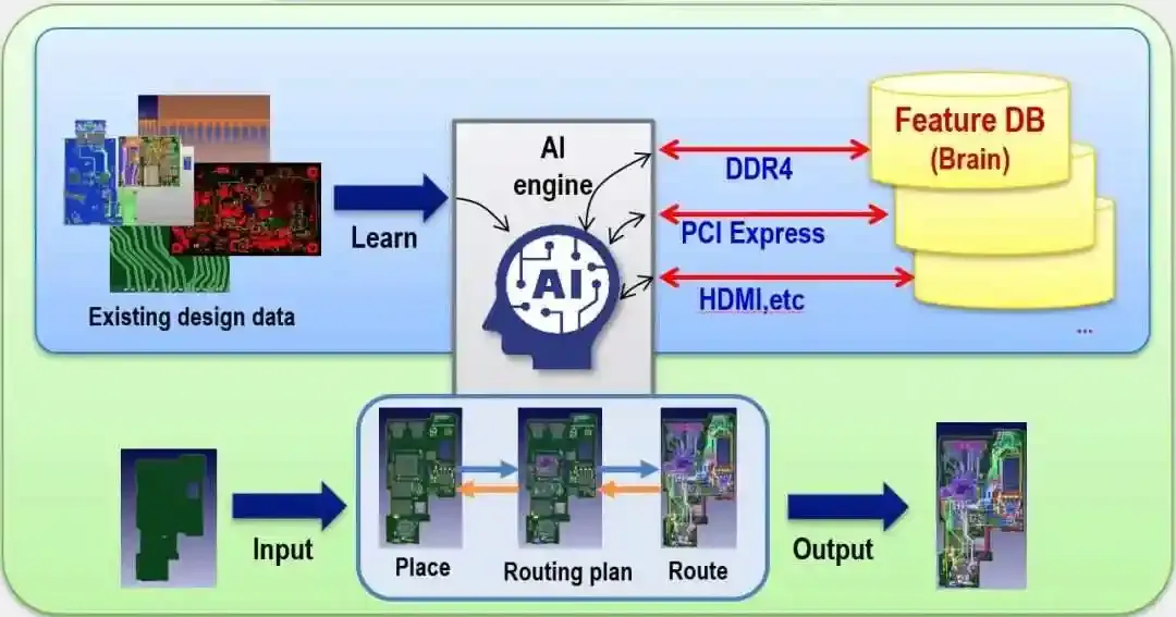
Artificial intelligence (AI) is revolutionizing many industries, and PCB design is no exception. AI tools are being used to optimize layouts, reduce design errors, and improve the efficiency of smart home PCBs. For instance, AI algorithms can analyze signal paths to minimize crosstalk and impedance mismatch, ensuring better performance in high-density designs.
In smart home applications, AI-driven design is particularly valuable for IoT devices that require complex routing and power management. By simulating thousands of design scenarios in minutes, AI helps engineers create PCBs that balance performance, cost, and size constraints. This trend is expected to grow as AI tools become more accessible, allowing even small design teams to tackle sophisticated projects.
Moreover, AI can predict potential failure points in a PCB design, such as thermal hotspots or signal bottlenecks, before manufacturing begins. This predictive capability reduces costly revisions and speeds up time-to-market for innovative smart home products.
Challenges in Adopting Future PCB Technologies
While these trends and innovations are exciting, they come with challenges that engineers must navigate. For example, embedded components require specialized manufacturing processes, which can increase upfront costs. Similarly, 3D printed electronics are not yet widely adopted for mass production, limiting their scalability for large smart home projects.
Biodegradable PCBs face hurdles in terms of performance and durability, as they may not yet match the reliability of traditional materials under harsh conditions. High-speed materials and AI tools, while powerful, often demand significant investment in equipment and training, which may be a barrier for smaller companies.
Despite these challenges, ongoing research and industry collaboration are steadily overcoming these obstacles. As technology matures, we expect costs to decrease and adoption to rise, making these innovations more accessible to all.
How These Trends Benefit Smart Home Engineers
For engineers working on smart home projects, staying ahead of PCB technology trends offers several advantages. Miniaturization and embedded components allow for more compact and efficient designs, enabling the creation of next-generation devices that stand out in a competitive market. 3D printed electronics provide flexibility and speed in prototyping, helping teams iterate faster and bring ideas to life.
Biodegradable PCBs align with the growing demand for sustainable products, appealing to eco-conscious consumers and regulators. High-speed materials ensure that devices meet the performance expectations of modern connectivity standards, while AI-driven design tools streamline workflows and reduce errors.
By embracing these innovations, engineers can create smart home solutions that are not only cutting-edge but also cost-effective and environmentally responsible. Staying informed about future PCB design trends is the key to maintaining a competitive edge in this fast-paced industry.
The Road Ahead for Smart Home PCBs
The future of smart home PCBs is bright, with innovations like embedded components, 3D printed electronics, and biodegradable materials leading the charge. As PCB technology trends continue to evolve, they will enable smarter, smaller, and more sustainable devices that enhance our daily lives. Whether it’s through faster connectivity, AI-optimized designs, or eco-friendly materials, the next generation of PCBs will play a crucial role in shaping the smart homes of tomorrow.
At ALLPCB, we’re committed to supporting engineers and designers with the tools and resources needed to bring these innovations to life. By staying at the forefront of PCB advancements, we aim to empower creators to build the future of smart home technology, one circuit board at a time.