ALLPCB


If you're an electrical engineer looking to design a reliable and efficient printed circuit board (PCB) with 1 oz copper, you're in the right place. This guide answers your key questions about 1 oz copper PCB current capacity, thermal management, and signal integrity right upfront. In short, 1 oz copper (equivalent to a thickness of 1.4 mils or 35 micrometers) can handle approximately 2-4 amps per 10 mils of trace width for a 10°C temperature rise, requires careful heat dissipation strategies like vias and heat sinks, and supports good signal integrity with proper trace spacing and grounding. Below, we dive deep into each aspect, including IPC-2221 trace width for 1 oz copper and practical tips for designing with 1 oz copper, to help you create robust PCB designs.
Introduction to 1 oz Copper in PCB Design
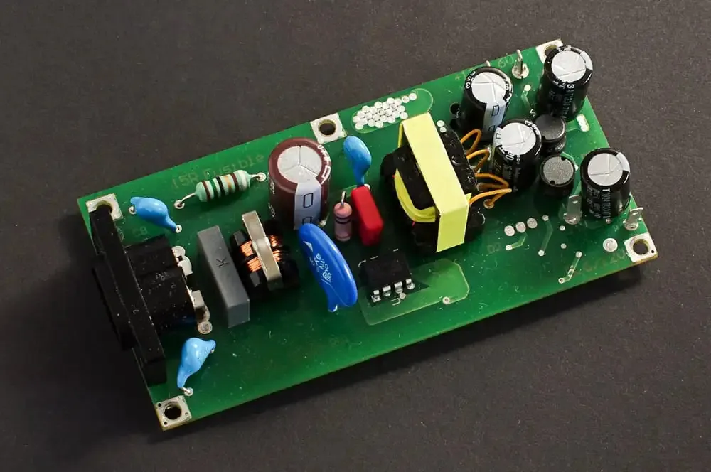
Designing a PCB with 1 oz copper is a common choice for many applications, from consumer electronics to industrial systems. The term "1 oz copper" refers to the weight of copper per square foot of the PCB, translating to a thickness of about 1.4 mils (35 micrometers). This thickness strikes a balance between cost, manufacturability, and performance, making it a go-to option for engineers. However, to get the most out of your design, you need to understand how 1 oz copper impacts current capacity, thermal behavior, and signal integrity.
In this guide, we'll break down each of these critical factors. Whether you're working on a high-power circuit or a high-speed digital design, you'll find actionable insights and data-driven tips tailored for electrical engineers. Let's start by exploring the current-carrying capacity of 1 oz copper PCBs.

Understanding 1 oz Copper PCB Current Capacity
One of the first questions engineers ask when designing with 1 oz copper is: how much current can it handle? The current capacity of a PCB trace depends on its width, the ambient temperature, and the acceptable temperature rise. For 1 oz copper, the general rule of thumb, based on the IPC-2221 standard, is that a 10-mil-wide trace can carry about 1 amp for a 10°C temperature rise in typical conditions.
However, for more accurate calculations, you can refer to the IPC-2221 trace width guidelines or use online calculators based on this standard. For instance, a 50-mil-wide trace on a 1 oz copper PCB can handle approximately 3-4 amps with a 10°C rise, assuming external traces in still air. If the trace is internal or in a hotter environment, the capacity drops due to reduced heat dissipation.
Here's a quick reference for 1 oz copper PCB current capacity (external traces, 10°C rise):
- 10 mil width: ~1 amp
- 20 mil width: ~1.5-2 amps
- 50 mil width: ~3-4 amps
Keep in mind that these values are conservative estimates. For high-current applications, consider increasing trace width or adding copper pours to distribute the load. Also, remember that stacking multiple layers of 1 oz copper doesn't proportionally increase capacity due to uneven current distribution, as noted in industry discussions on platforms like X.
Thermal Management in 1 oz Copper PCB Designs
Thermal management is a critical concern when working with 1 oz copper, especially in high-power designs. The relatively thin copper layer means heat dissipation can be challenging compared to thicker options like 2 oz or 3 oz copper. Poor 1 oz copper PCB thermal management can lead to hotspots, component failure, or reduced lifespan of the board.
Here are some practical strategies for managing heat in your 1 oz copper PCB designs:
- Use Thermal Vias: Place thermal vias under heat-generating components like power ICs or MOSFETs to transfer heat to other layers or a heat sink. A grid of 0.3 mm vias spaced 1.2 mm apart can significantly improve heat dissipation.
- Add Copper Pours: Large copper areas connected to ground or power planes can act as heat spreaders. Ensure these pours are uninterrupted by cuts or slots for maximum effect.
- Optimize Component Placement: Position high-power components near board edges or areas with better airflow to avoid centralized heat buildup.
- Consider External Cooling: For demanding applications, attach heat sinks or use forced air cooling. Ensure thermal pads or paste are used for good contact.
According to the IPC-2152 standard, which updates thermal considerations from IPC-2221, trace temperature rise is directly tied to current and board design. For a 1 oz copper trace carrying 3 amps on a 50-mil width, you might see a temperature rise of 10-20°C above ambient without proper cooling. Use simulation tools or calculators aligned with IPC-2152 to predict and mitigate thermal issues early in the design phase.

Ensuring Signal Integrity with 1 oz Copper PCBs
Signal integrity is another crucial aspect of PCB design, especially for high-speed digital or RF applications. While 1 oz copper is suitable for many designs, its thickness and the resulting trace geometry can impact signal performance if not handled correctly. Let's explore how to maintain 1 oz copper PCB signal integrity.
Trace Impedance Control: For high-speed signals, maintaining consistent impedance (often 50 ohms for RF or 100 ohms differential for high-speed digital) is essential. With 1 oz copper, trace width and dielectric thickness determine impedance. For a standard FR-4 substrate with a 1.6 mm thickness, a 50-ohm single-ended trace might require a width of about 60 mils. Use impedance calculators or simulation software to fine-tune these values.
Minimizing Crosstalk: Crosstalk occurs when adjacent traces interfere with each other. To reduce this, maintain adequate spacing—typically 3x the trace width for critical signals. For example, a 10-mil trace should have at least 30 mils of separation from neighboring traces.
Ground Planes: A solid ground plane beneath signal traces helps reduce noise and provides a return path for high-frequency signals. Avoid using copper pours with slots or cuts under high-speed traces, as this can disrupt the return path and increase electromagnetic interference (EMI), a concern highlighted in recent industry posts on social platforms.
For designs operating above 100 MHz, consider controlled impedance routing and ensure minimal via stubs, as they can act as antennas and degrade signal quality. If your design pushes the limits of 1 oz copper, you might need to explore thinner dielectrics or multilayer boards for better control.

Applying IPC-2221 Standards for Trace Width in 1 oz Copper Designs
The IPC-2221 standard is a cornerstone for PCB design, providing guidelines for trace width, spacing, and other parameters to ensure reliability. When designing with 1 oz copper, adhering to IPC-2221 trace width for 1 oz copper is crucial for balancing current capacity and thermal performance.
IPC-2221 provides charts and formulas to calculate trace width based on current, temperature rise, and copper thickness. For a 1 oz copper PCB, the standard suggests the following approximate trace widths for a 10°C temperature rise (external traces):
- 1 amp: 10 mils
- 2 amps: 20-25 mils
- 3 amps: 35-40 mils
These values assume standard conditions (25°C ambient, still air). For internal traces or higher ambient temperatures, you’ll need wider traces or additional cooling measures. The standard also accounts for voltage spacing (clearance and creepage) to prevent arcing, which is critical in high-voltage designs.
While IPC-2221 is widely used, note that the newer IPC-2152 standard offers updated thermal models based on more recent testing. Many engineers use tools and calculators aligned with both standards to cross-verify their designs. Resources like those from Altium or Sierra Circuits can help you apply these standards effectively.
Practical Tips for Designing with 1 oz Copper
Now that we've covered the technical foundations, let’s look at some hands-on tips for designing with 1 oz copper. These are drawn from industry best practices and real-world experience to help you avoid common pitfalls.
- Start with Simulation: Use PCB design software like Altium Designer or KiCad to simulate current flow and thermal behavior before fabrication. This can catch issues like insufficient trace width or potential hotspots early.
- Plan for Manufacturability: Stick to standard trace widths and spacings (e.g., 6-8 mils minimum for most fabricators) to avoid production issues. Check with your PCB manufacturer for their specific capabilities with 1 oz copper.
- Balance Cost and Performance: While 1 oz copper is cost-effective, don’t hesitate to move to 2 oz copper for high-current areas if budget allows. Alternatively, use wider traces or multiple layers to compensate.
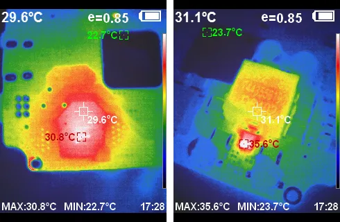
- Test Prototypes: Always build and test a prototype under real-world conditions. Measure temperature rise with an infrared camera and check signal integrity with an oscilloscope to validate your design.
I recall a project where I designed a power supply board with 1 oz copper, initially underestimating the current on a key trace. After simulation showed a 30°C rise, I doubled the trace width and added thermal vias, dropping the rise to under 10°C. Small adjustments like this, guided by standards and tools, can make a big difference.
Common Challenges and How to Overcome Them
Designing with 1 oz copper isn’t without challenges. Here are some frequent issues and solutions:
- Overheating: If traces overheat, widen them or add copper pours. For extreme cases, integrate heat sinks or fans.
- Signal Noise: High-speed designs may suffer from noise or crosstalk. Route critical traces away from noisy areas and use ground planes effectively.
- Manufacturing Limits: Some fabricators struggle with fine traces on 1 oz copper. Confirm their minimum trace width and spacing (often 6 mils) before finalizing your design.
By anticipating these issues and planning ahead, you can save time and costly redesigns. Always iterate on your design with feedback from simulations and prototype testing.
Conclusion: Mastering 1 oz Copper PCB Design
Designing a PCB with 1 oz copper offers a cost-effective and versatile solution for many applications, but it demands careful attention to 1 oz copper PCB current capacity, thermal management, and signal integrity. By following guidelines like IPC-2221 trace width for 1 oz copper and applying practical tips for designing with 1 oz copper, you can create reliable and efficient boards tailored to your needs.
Remember to use simulation tools, adhere to industry standards, and test prototypes to validate your designs. Whether you're managing high currents or ensuring clean signals, the strategies in this guide will help you succeed. Have questions or experiences to share? Drop a comment below—we’d love to hear how you’ve tackled challenges with 1 oz copper PCBs!