 ALLPCB


If you're looking for reliable solutions for 6-layer PCB prototyping services with quick turnaround and thorough design validation, you've come to the right place. At ALLPCB, we specialize in delivering high-quality 6-layer PCB prototypes fast, ensuring your designs are validated and ready for production. In this blog, we'll dive deep into the process of prototyping 6-layer PCBs, the importance of quick turn services, and how design validation and iteration can save time and costs. Whether you're an engineer working on complex electronics or a startup racing to market, this guide will provide actionable insights to streamline your project.
Why Choose 6-Layer PCBs for Your Project?
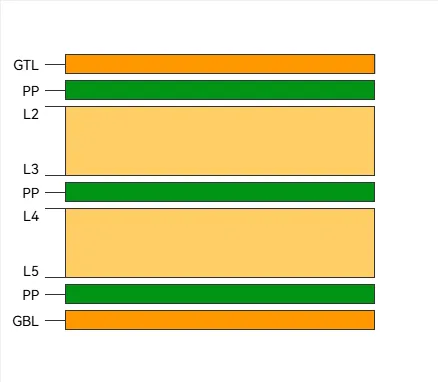
6-layer PCBs are a popular choice for advanced electronic designs that require higher density and better performance than simpler 2- or 4-layer boards can provide. These boards consist of six conductive layers, typically used for power distribution, ground planes, and signal routing. They are ideal for applications like telecommunications, medical devices, and industrial controls where space is limited, and functionality is critical.
With a 6-layer PCB, you can achieve better signal integrity by dedicating specific layers to ground and power planes, reducing electromagnetic interference (EMI). For instance, a typical configuration might include two outer signal layers, two internal power/ground planes, and two additional signal layers in the middle. This setup can support high-speed signals up to 5 GHz in some designs, depending on the materials and stack-up used. The ability to route complex circuits in a compact form factor makes 6-layer PCBs essential for modern electronics.
The Importance of 6-Layer PCB Prototyping Services
Prototyping is a crucial step in the development of any electronic product. For 6-layer PCBs, prototyping services allow engineers to test their designs before committing to full-scale production. This phase helps identify issues like incorrect trace routing, impedance mismatches, or thermal problems that could lead to costly redesigns later.
Using professional 6-layer PCB prototyping services ensures that your boards are manufactured with precision, adhering to tight tolerances for layer alignment and via placement. For example, a typical 6-layer board may require controlled impedance traces with a tolerance of ±10% to maintain signal integrity at high frequencies. Prototyping also allows you to verify the stack-up design, ensuring that dielectric thicknesses (often around 0.1 mm to 0.2 mm between layers) meet your specifications for performance.
At ALLPCB, we focus on delivering prototypes that meet these exacting standards, helping you move from concept to testing in the shortest time possible. Our services are tailored to handle the complexities of multilayer boards, ensuring your project stays on track.
6-Layer PCB Quick Turn: Speed Without Compromise
Time is often a critical factor in product development. That's where 6-layer PCB quick turn services come into play. These services are designed to provide rapid fabrication and assembly, sometimes delivering prototypes in as little as 24 to 48 hours for urgent projects. This speed is essential for industries like consumer electronics, where getting to market first can make or break a product launch.
Quick turn services for 6-layer PCBs don't mean cutting corners. Advanced manufacturing processes, such as automated optical inspection (AOI) and X-ray testing for internal layers, ensure that even fast-tracked boards meet quality standards. For instance, via drilling for a 6-layer board requires precision to avoid misalignment, with diameters often as small as 0.2 mm for microvias. Our commitment at ALLPCB is to balance speed with reliability, so you can test your designs without delay.
6-Layer PCB Design Validation: Ensuring Success Before Production
Design validation is a critical part of the prototyping process, especially for complex 6-layer PCBs. This step involves checking every aspect of your design to ensure it functions as intended under real-world conditions. Without proper validation, small errors—like a misrouted trace or an unbalanced power plane—can lead to performance issues or complete failure.
For 6-layer PCB design validation, engineers often focus on several key areas:
- Signal Integrity: Ensuring high-speed signals maintain their quality across layers. For example, a differential pair on a 6-layer board might require a specific impedance of 100 ohms ±5% to avoid signal loss.
- Power Distribution: Verifying that power and ground planes provide stable voltage and current, minimizing noise. A common issue is insufficient decoupling capacitors, which can be caught during validation.
- Thermal Management: Checking for hotspots that could affect component reliability. Thermal vias and proper copper thickness (e.g., 1 oz or 2 oz per square foot) are often analyzed.
At ALLPCB, we support design validation by offering detailed feedback during the prototyping phase. Our team can assist in identifying potential issues before they become costly problems, ensuring your 6-layer PCB is ready for the next stage.
6-Layer PCB Prototype Testing: From Theory to Reality
Once your 6-layer PCB prototype is fabricated, testing becomes the next critical step. 6-Layer PCB prototype testing involves putting the board through a series of evaluations to confirm that it meets design specifications and performs reliably in its intended application.
Common testing methods include:
- Functional Testing: Verifying that the board operates as expected under normal conditions. This might involve powering up the board and checking for correct voltage levels at key points.
- Environmental Testing: Subjecting the PCB to temperature and humidity variations to simulate real-world conditions. For example, testing at temperatures from -40°C to 85°C can reveal potential weaknesses.
- Signal Testing: Using oscilloscopes to measure signal rise times and jitter, especially for high-speed designs. A rise time of less than 1 ns might be required for certain applications.
Testing at the prototype stage helps catch issues early, saving significant time and resources. Our prototyping services at ALLPCB are designed to support thorough testing, providing you with boards that are ready for rigorous evaluation.
6-Layer PCB Design Iteration: Refining for Perfection
Design iteration is often necessary after initial prototype testing. Rarely does a first design work flawlessly, especially with the complexity of 6-layer PCBs. 6-Layer PCB design iteration involves analyzing test data, identifying areas for improvement, and updating the design accordingly.
For example, if testing reveals excessive crosstalk between adjacent traces, you might need to adjust the spacing or add a ground plane shield. If thermal issues are detected, increasing the copper weight or adding more vias for heat dissipation could be the solution. Each iteration brings the design closer to perfection, ensuring reliability and performance in the final product.
At ALLPCB, we understand the importance of rapid design iteration. Our quick turn services allow you to receive updated prototypes quickly, so you can test and refine without losing momentum. This iterative approach is key to achieving a market-ready product in the shortest possible time.
Benefits of Partnering with ALLPCB for 6-Layer PCB Prototyping
Choosing the right partner for your 6-layer PCB prototyping needs can make all the difference. At ALLPCB, we offer a range of benefits tailored to engineers and businesses working on complex multilayer designs:
- Fast Turnaround Times: Our streamlined processes ensure you receive prototypes in record time, often within days, without sacrificing quality.
- Expert Support: Our team provides guidance on design validation and iteration, helping you avoid common pitfalls.
- Advanced Manufacturing: We use state-of-the-art equipment to handle the precision requirements of 6-layer PCBs, such as microvia drilling and controlled impedance.
- Cost-Effective Solutions: Prototyping with us helps you save on redesign costs by catching issues early, keeping your project within budget.
Our goal is to support your success by delivering prototypes that meet your exact specifications, on time and ready for testing.
Best Practices for Designing 6-Layer PCBs for Prototyping
To make the most of 6-layer PCB prototyping services, consider these best practices during the design phase:
- Plan Your Stack-Up Carefully: Dedicate layers for power and ground to minimize noise. A common stack-up might be signal-ground-power-power-ground-signal.
- Optimize Via Placement: Use blind and buried vias strategically to save space, but avoid overuse as they can increase fabrication costs.
- Simulate Before Prototyping: Use simulation tools to predict signal integrity and thermal performance, reducing the number of physical iterations needed.
- Follow Design Rules: Adhere to manufacturing design rules for trace widths (e.g., minimum 0.1 mm for high-density designs) and spacing to ensure manufacturability.
By incorporating these practices, you can streamline the prototyping process and achieve better results with fewer revisions.
Conclusion: Streamline Your Project with 6-Layer PCB Prototyping
Prototyping 6-layer PCBs is a vital step in bringing complex electronic designs to life. With the right 6-layer PCB prototyping services, quick turn capabilities, and a focus on design validation, testing, and iteration, you can ensure your project stays on track and meets performance goals. At ALLPCB, we're committed to providing fast, reliable solutions that help engineers and businesses succeed in competitive markets.
From tackling signal integrity challenges to refining designs through iterative testing, our expertise in 6-layer PCB quick turn and design validation ensures you get high-quality prototypes without delay. Trust us to be your partner in turning innovative ideas into reality, delivering boards that are ready for the next phase of development.


