 ALLPCB


If you're new to PCB design or manufacturing and wondering how to ensure precise component placement during assembly, panel fiducials are the answer. These small but critical markers help machines align printed circuit boards (PCBs) accurately during the surface mount technology (SMT) process. In this beginner's guide, we'll explore the basics of panel fiducials, their role in PCB alignment, and how they contribute to a smooth manufacturing process. Whether you're looking for a PCB alignment guide or a fiducial mark tutorial, this post will walk you through everything you need to know about panel fiducial basics and SMT alignment.
What Are Panel Fiducials and Why Do They Matter?
Panel fiducials are small reference points or markers placed on a PCB or a panel of multiple PCBs. These markers, often made of exposed copper in a circular shape, act as visual guides for automated assembly machines. During the PCB manufacturing process, machines like pick-and-place systems and stencil printers use fiducials to determine the exact position and orientation of the board. Without these markers, even a slight misalignment could lead to misplaced components, resulting in defective products.
Fiducials are especially important when dealing with panels—large sheets containing multiple PCBs. They ensure that every board on the panel is aligned correctly during SMT assembly. For beginners, understanding panel fiducial basics can save time, reduce errors, and improve the overall quality of your PCB projects.

The Role of Fiducials in PCB Alignment
PCB alignment is a critical step in the manufacturing process, especially during SMT assembly, where components are placed on the board with micron-level precision. Fiducial marks serve as reference points for the vision systems in automated machines. These systems capture images of the fiducials to calculate the board's position and orientation, adjusting their operations accordingly.
There are typically two types of fiducials used for alignment:
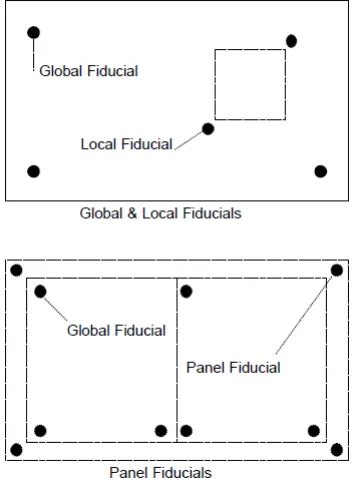
- Global Fiducials: These are placed on the panel or board to provide an overall reference for the entire layout. They help machines understand the general orientation of the panel. Usually, at least two global fiducials are placed on opposite corners of the panel, ensuring a reliable reference for the machine’s vision system.
- Local Fiducials: These are placed near specific components or areas on individual PCBs within the panel. They are used for fine-tuning alignment in high-precision areas, especially for components with tight tolerances, like fine-pitch ICs or BGA (Ball Grid Array) packages.
By using both types of fiducials, manufacturers can achieve accuracy down to 0.01mm or better, depending on the equipment. This level of precision is crucial for modern electronics, where even a small error can lead to signal integrity issues or complete circuit failure.
How Fiducial Marks Work in SMT Alignment
SMT alignment is the process of ensuring that components are placed exactly where they belong on a PCB. During assembly, a pick-and-place machine uses cameras to locate fiducial marks on the board. These marks act like a map, telling the machine where the board starts and how it’s oriented. Here’s a simplified step-by-step breakdown of how it works:
- The PCB or panel is loaded into the SMT machine.
- The machine’s vision system scans the board to find the fiducial marks.
- Using the position of the fiducials, the machine calculates the board’s exact location and any rotational offset (e.g., if the board is slightly tilted).
- The machine adjusts its placement coordinates based on this data, ensuring components are placed accurately.
Without fiducials, the machine would rely on less reliable methods like board edges, which can vary in shape or position due to manufacturing tolerances. Fiducials provide a consistent and precise reference, making them indispensable for high-speed, automated assembly.
Panel Fiducial Basics: Design and Placement Tips
For those just starting with PCB design, getting fiducial marks right is essential for a smooth manufacturing process. Here are some key tips and best practices for designing and placing fiducials on your PCB panel:
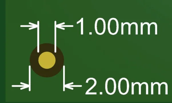
1. Shape and Size of Fiducials
Fiducial marks are typically circular, with a diameter of 1mm to 3mm, depending on the machine’s vision system requirements. The mark should be made of exposed copper, free of solder mask, to ensure maximum contrast for the camera. Around the fiducial, there should be a clearance area (also free of solder mask) at least twice the diameter of the mark itself. This prevents interference from nearby features and ensures the camera can detect the fiducial clearly.
2. Number and Location of Fiducials
For global alignment on a panel, place at least two fiducials on opposite corners, ideally as far apart as possible. Three fiducials are even better, as they provide additional data for correcting rotational errors. For local alignment, add fiducials near high-precision components, ensuring they’re within the camera’s field of view for that specific area.
3. Avoid Symmetry in Placement
Place fiducials asymmetrically to avoid confusion for the machine. If fiducials are placed symmetrically, the vision system might misinterpret the board’s orientation, leading to a 180-degree rotation error. For example, on a rectangular panel, position two fiducials on one side and the third on the opposite side, creating a unique triangle pattern.
4. Check Manufacturer Guidelines
Different assembly machines may have specific requirements for fiducial design and placement. Always consult the guidelines provided by your manufacturing partner to ensure compatibility with their equipment. This can prevent costly delays or rework during production.
Fiducials in the PCB Manufacturing Process
Fiducials play a role throughout the PCB manufacturing process, not just during SMT assembly. Here’s how they contribute at different stages:
1. Stencil Printing
Before components are placed, solder paste is applied to the PCB using a stencil. Fiducials help align the stencil with the board, ensuring that paste is deposited precisely where pads are located. Misalignment at this stage can lead to soldering defects like bridges or insufficient paste.
2. Component Placement
As discussed earlier, fiducials are critical for pick-and-place machines to position components accurately. For high-density designs with components spaced less than 0.5mm apart, even a tiny error can cause shorts or open circuits.
3. Inspection and Testing
After assembly, automated optical inspection (AOI) systems use fiducials to verify component placement and detect defects. Fiducials help these systems map the board’s layout, ensuring that every component is checked against the design data.
By incorporating well-designed fiducials, you streamline the entire manufacturing process, from paste application to final inspection, reducing the risk of errors at every step.
Common Mistakes to Avoid with Panel Fiducials
Even with a basic understanding of fiducials, beginners often make mistakes that can disrupt the PCB manufacturing process. Here are some pitfalls to watch out for:
- Covering Fiducials with Solder Mask: If a fiducial is accidentally covered by solder mask, the machine’s camera may not detect it, leading to alignment failures. Always ensure fiducials and their surrounding clearance areas are free of any coating.
- Placing Fiducials Too Close to Edges: Fiducials near the board edge may be damaged during depanelization (separating individual PCBs from the panel). Keep them at least 5mm away from edges or breakaway tabs.
- Ignoring Local Fiducials for Complex Designs: For boards with fine-pitch components (e.g., 0.4mm pitch QFN packages), skipping local fiducials can result in placement errors. Add local markers near critical areas to ensure precision.
- Using Inconsistent Fiducial Sizes: If fiducials on the same panel vary in size or shape, it can confuse the vision system. Stick to a uniform design for all fiducials on a single panel.
Avoiding these mistakes can save you from costly rework and ensure a smoother SMT alignment process.
Benefits of Proper Fiducial Placement for SMT Assembly
Investing time in proper fiducial design and placement offers several advantages during PCB assembly:
- Improved Accuracy: Fiducials enable placement precision down to 0.01mm, critical for modern high-density designs.
- Faster Production: With clear reference points, machines can align and place components quickly, reducing cycle times.
- Reduced Errors: Accurate alignment minimizes defects like misaligned components or solder bridges, lowering rework costs.
- Compatibility with Automation: Fiducials ensure seamless integration with automated systems, supporting high-volume production.
For beginners, mastering fiducial placement is a small step that yields big returns in terms of product quality and manufacturing efficiency.
How to Incorporate Fiducials in Your PCB Design Software
Most PCB design tools allow you to add fiducial marks easily during the layout phase. Here’s a general guide to incorporating them:
- Open your PCB layout editor and navigate to the layer where fiducials will be placed (usually the top or bottom copper layer).
- Create a circular pad with a diameter of 1mm to 3mm, ensuring it’s free of solder mask by adding a corresponding shape in the solder mask layer.
- Define a clearance area around the fiducial, typically 2 to 3 times the diameter of the mark, also free of solder mask.
- Place the fiducials in strategic locations on the panel or board, following the guidelines for global and local markers.
- Label the fiducials in your design files (e.g., “FID1,” “FID2”) to make them easily identifiable during manufacturing.
Double-check your design files before sending them to your manufacturing partner to ensure all fiducials are correctly defined and positioned. Many design tools also offer DRC (Design Rule Check) features to verify fiducial placement against standard requirements.
Conclusion: Mastering PCB Alignment with Panel Fiducials
Panel fiducials are a small but powerful tool in the world of PCB design and manufacturing. By understanding panel fiducial basics and following best practices for placement and design, you can ensure precise SMT alignment and streamline the entire PCB manufacturing process. Whether you’re a beginner or an experienced engineer, this PCB alignment guide serves as a starting point to improve the quality and efficiency of your projects.
From global fiducials that provide overall panel orientation to local fiducials that fine-tune precision for critical components, these markers are essential for modern electronics assembly. Take the time to incorporate them into your designs, avoid common mistakes, and consult with your manufacturing partner for specific requirements. With the right approach, fiducials will help you achieve flawless PCB alignment every time.


