 ALLPCB


If you're looking to ensure the highest quality in printed circuit board (PCB) manufacturing, mastering microsectioning is essential. This process, often referred to as cross-sectioning, is a critical step in PCB quality control that helps detect hidden defects and verify structural integrity. In this guide, we’ll explore microsectioning PCB quality control steps, microsectioning for PCB defect detection, and broader PCB quality inspection methods to help you achieve reliable and high-performing boards.
Whether you're an engineer, quality control specialist, or manufacturer, this comprehensive resource will walk you through the why, how, and what of microsectioning, providing actionable insights to elevate your PCB production process.
Why Microsectioning Matters in PCB Quality Control
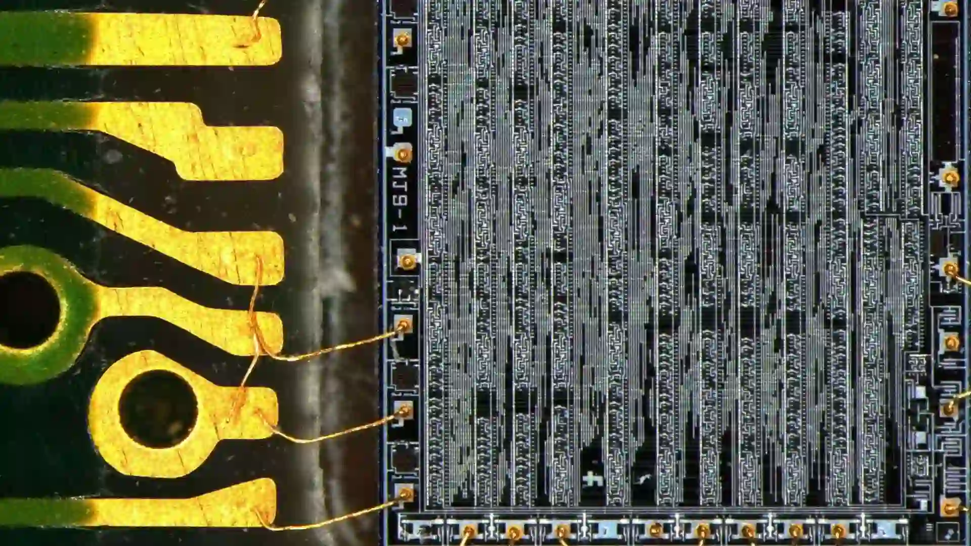
In the world of electronics, even the smallest defect in a PCB can lead to catastrophic failures, from short circuits to complete device malfunctions. Microsectioning is a destructive testing method that involves cutting a small section of a PCB to examine its internal structure under a microscope. This technique reveals issues that are invisible to the naked eye or even advanced non-destructive testing methods like X-ray inspection.
By using microsectioning, manufacturers can identify problems such as delamination, voids in solder joints, uneven copper plating, or misaligned layers. For instance, a void in a plated through-hole (PTH) might weaken electrical connectivity, increasing resistance beyond acceptable levels (e.g., above 10 milliohms for high-reliability applications). Detecting such issues early ensures that defective boards don't make it to the final product, saving time, cost, and reputation.
What Is Microsectioning in PCB Manufacturing?
Microsectioning is a detailed process where a small sample of a PCB is cut, mounted, polished, and examined under high magnification. This method provides a clear view of the board's internal features, including the copper traces, dielectric layers, vias, and solder joints. It is often guided by industry standards like IPC-6012, which specifies acceptable limits for defects in rigid printed boards.
The primary goal of microsectioning is to validate the manufacturing process and ensure that the PCB meets design specifications. For example, it can confirm whether the copper thickness in a via meets the required minimum of 25 micrometers for Class 3 high-reliability boards, as per IPC standards. If the thickness is below this threshold, the board may fail under thermal or mechanical stress.
Key Benefits of Microsectioning for PCB Defect Detection
Microsectioning offers several advantages that make it indispensable for quality control in PCB manufacturing. Here are some of the key benefits:
- Reveals Hidden Defects: Issues like internal cracks, voids, or delamination that can't be detected through surface inspection are easily identified.
- Validates Manufacturing Processes: It ensures that processes like drilling, plating, and lamination are performed correctly, maintaining consistency across batches.
- Improves Reliability: By catching defects early, microsectioning helps prevent failures in critical applications, such as aerospace or medical devices.
- Supports Failure Analysis: When a PCB fails in the field, microsectioning can pinpoint the root cause, whether it's poor soldering or material defects.
Microsectioning PCB Quality Control Steps
Performing microsectioning correctly requires precision and adherence to a structured process. Below are the essential steps to ensure accurate results and effective quality control:
1. Sample Selection and Preparation
The first step is to select a representative sample from the batch of PCBs. This could be a board from the beginning, middle, or end of a production run to ensure comprehensive coverage. Once selected, the sample is cut into a smaller piece using a precision saw to avoid damaging the internal structure. The cut should be made at a location of interest, such as near a via or a solder joint, to inspect specific features.
2. Mounting the Sample
After cutting, the sample is mounted in a resin or epoxy material to hold it securely during polishing. This step prevents the delicate layers of the PCB from shifting or breaking apart. The mounting material is cured, typically for 24-48 hours, to create a solid block that can be handled easily.
3. Grinding and Polishing
The mounted sample is then ground and polished to create a smooth, flat surface for microscopic examination. This process starts with coarse abrasives (e.g., 120-grit sandpaper) to remove excess material and progresses to finer abrasives (up to 1200-grit or higher) for a mirror-like finish. Proper polishing is crucial to avoid scratches that could obscure defects.
4. Etching (Optional)
In some cases, the polished surface is etched with a chemical solution to enhance the visibility of certain features, such as copper grain boundaries or solder interfaces. For instance, a mild acid etch can highlight uneven plating in a via, making it easier to measure thickness under a microscope.
5. Microscopic Examination
The prepared sample is examined under a high-powered microscope, often at magnifications ranging from 50x to 1000x, depending on the feature being inspected. Measurements are taken to verify dimensions, such as the thickness of copper layers (e.g., ensuring a minimum of 1 mil or 25.4 micrometers for inner layers). Defects like voids, cracks, or delamination are documented with images for reporting.
6. Reporting and Analysis
Finally, the findings are compiled into a detailed report that includes measurements, observations, and photographic evidence of any defects. This report is used to determine whether the batch meets quality standards or if corrective actions are needed in the manufacturing process.
Common Defects Detected Through Microsectioning
Microsectioning is particularly effective for identifying internal defects that could compromise PCB performance. Here are some of the most common issues it uncovers:
- Voids in Plated Through-Holes (PTHs): Voids can increase electrical resistance, often exceeding acceptable limits (e.g., 5-10 milliohms), leading to signal integrity issues.
- Delamination: Separation between layers can weaken the board's structure, especially under thermal stress, causing failures in high-temperature environments.
- Uneven Copper Plating: Insufficient or excessive plating in vias or traces can result in poor conductivity or short circuits.
- Cracks in Solder Joints: Micro-cracks can grow over time, especially in applications with frequent thermal cycling, leading to open circuits.
- Misaligned Layers: Improper registration during lamination can cause signal paths to deviate, affecting high-speed performance (e.g., impedance mismatches beyond ±10% of the target value).
Broader PCB Quality Inspection Methods
While microsectioning is a powerful tool for defect detection, it is just one part of a comprehensive PCB quality control strategy. Combining it with other inspection methods ensures a higher level of reliability. Below are some complementary PCB quality inspection methods to consider:
1. Visual Inspection
Visual inspection is the first line of defense, often performed manually or with automated optical inspection (AOI) systems. It checks for surface-level defects like scratches, misprints, or missing components. While it can't detect internal issues, it's a quick way to catch obvious problems early.
2. X-Ray Inspection
X-ray inspection is a non-destructive method that can reveal hidden defects like voids in solder joints or misaligned components in multilayer boards. It's especially useful for inspecting ball grid array (BGA) connections without cutting the board.
3. Electrical Testing
Electrical tests, such as in-circuit testing (ICT) and flying probe testing, verify the functionality of the PCB by checking for shorts, opens, and correct impedance values (e.g., ensuring a 50-ohm impedance for high-speed signals). These tests are essential for confirming that the board performs as designed.
4. Thermal Imaging
Thermal imaging detects hot spots on a powered PCB, which could indicate high-resistance areas or poor solder joints. For instance, a temperature rise above 20°C in a specific area might suggest a defect that needs further investigation through microsectioning.
Best Practices for Effective Microsectioning
To get the most out of microsectioning, follow these best practices to ensure accuracy and reliability:
- Use Proper Equipment: Invest in high-quality cutting, polishing, and microscopy tools to avoid introducing artifacts or damage during preparation.
- Adhere to Standards: Follow industry guidelines like IPC-A-600 for acceptability criteria and IPC-TM-650 for test methods to maintain consistency.
- Train Personnel: Ensure that staff are well-trained in sample preparation and defect identification to minimize errors.
- Document Everything: Keep detailed records of each microsectioning analysis, including images and measurements, for traceability and future reference.
- Combine with Other Tests: Use microsectioning alongside non-destructive methods to get a complete picture of PCB quality without sacrificing too many boards.
Challenges in Microsectioning and How to Overcome Them
While microsectioning is highly effective, it does come with challenges. One major drawback is that it is a destructive test, meaning the tested sample cannot be used afterward. To address this, select only a small percentage of boards for testing, focusing on critical or high-risk areas.
Another challenge is the time and cost involved. Preparing and analyzing a single sample can take several hours, and the equipment can be expensive. To mitigate this, prioritize microsectioning for high-reliability applications or during process validation rather than routine production checks.
Finally, interpreting the results requires expertise. Misidentifying a defect or overlooking a subtle issue can lead to incorrect conclusions. Regular training and calibration of equipment can help maintain accuracy.
Conclusion: Elevating PCB Quality with Microsectioning
Microsectioning is a cornerstone of effective PCB quality control, offering unparalleled insight into the internal structure of a board. By following the detailed microsectioning PCB quality control steps outlined in this guide, you can ensure that defects are caught early, processes are validated, and reliability is maintained. When combined with other PCB quality inspection methods, microsectioning becomes even more powerful, providing a robust framework for producing high-quality boards.


