 ALLPCB


When designing an 8-layer PCB stackup, selecting the right materials is critical to ensure performance, reliability, and cost-effectiveness for your specific application. Whether you're working on high-frequency circuits, power electronics, or standard digital designs, the choice between materials like FR-4 and high-frequency laminates can make or break your project. In this comprehensive guide, we’ll explore the key factors in material selection for an 8-layer PCB, compare popular options, and provide actionable insights to help you make an informed decision.
At its core, the decision often comes down to balancing electrical performance, thermal management, and budget. For standard applications, FR-4 is a reliable and cost-effective choice, while high-frequency designs may require advanced laminates with lower dielectric constants and loss tangents. Let’s dive deeper into the specifics of 8-layer PCB material selection, focusing on dielectric properties, stackup configurations, and application needs.
Why Material Selection Matters for 8-Layer PCB Stackups
An 8-layer PCB stackup offers significant design flexibility, allowing for complex routing, better signal integrity, and improved power distribution. However, with multiple layers comes the challenge of managing signal loss, impedance control, and thermal dissipation—all of which are heavily influenced by the materials used. The dielectric material between copper layers affects how signals propagate, while the overall stackup design impacts crosstalk and electromagnetic interference (EMI).
Choosing the wrong material can lead to issues like signal degradation, overheating, or even board failure. For instance, in high-frequency applications operating above 1 GHz, a material with a high dielectric constant or loss tangent can cause significant signal attenuation. On the other hand, using an expensive high-performance laminate for a low-frequency design may unnecessarily inflate costs. Understanding your application’s requirements is the first step in making the right choice for an 8-layer PCB stackup.
Key Factors in 8-Layer PCB Material Selection
Before comparing specific materials, let’s break down the critical factors to consider when selecting materials for an 8 layer PCB. These properties will guide your decision based on the demands of your project.
1. Dielectric Constant (Dk)
The dielectric constant, often abbreviated as Dk, measures how much a material can store electrical energy in an electric field. For an 8-layer PCB, the Dk value impacts signal speed and impedance. Materials with a lower Dk are preferred for high-frequency designs because they allow signals to travel faster with less delay. For example, a typical FR-4 material has a Dk of around 4.3 to 4.5, while advanced laminates can have Dk values as low as 2.2 to 3.5.
2. Dissipation Factor (Df) or Loss Tangent
The dissipation factor (Df) indicates how much signal energy is lost as heat in the material. A lower Df is crucial for high-frequency applications to minimize signal loss. FR-4 typically has a Df of 0.02, which is acceptable for low to mid-frequency designs but can cause significant losses above 1 GHz. High-frequency materials often have a Df below 0.005, making them ideal for RF and microwave circuits.
3. Thermal Stability
In an 8-layer PCB, heat dissipation across multiple layers is a concern, especially for power-intensive applications. Materials with good thermal stability maintain their properties under high temperatures. FR-4 can handle temperatures up to about 130°C, while some high-frequency laminates can withstand over 200°C, ensuring reliability in harsh environments.
4. Cost and Manufacturability
Budget constraints often play a big role in material selection. Standard materials like FR-4 are widely available and cost-effective, making them suitable for most general-purpose 8-layer PCBs. High-performance laminates, while superior in electrical and thermal properties, can be significantly more expensive and may require specialized manufacturing processes.
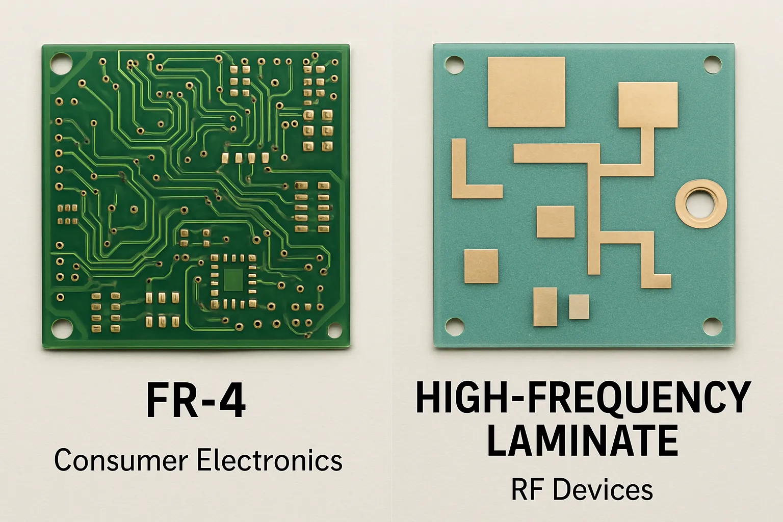
8-Layer PCB FR-4 vs. High-Frequency Laminates: A Detailed Comparison
Two of the most common material categories for 8-layer PCBs are FR-4 and high-frequency laminates. Let’s compare these options across key parameters to help you decide which is best for your application.
FR-4: The Standard Choice for 8-Layer PCBs
FR-4 is a fiberglass-reinforced epoxy laminate that serves as the industry standard for PCB substrates. It’s widely used due to its affordability, durability, and decent electrical properties for many applications.
- Dielectric Constant (Dk): Around 4.3–4.5, suitable for low to mid-frequency designs (up to 1 GHz).
- Dissipation Factor (Df): Approximately 0.02, leading to higher signal loss in high-frequency applications.
- Thermal Stability: Good up to 130°C, but performance degrades at higher temperatures.
- Cost: Low, making it ideal for cost-sensitive projects.
- Applications: Best for digital circuits, power supplies, and consumer electronics where high-frequency performance isn’t critical.
High-Frequency Laminates: Optimized for RF and Microwave
High-frequency laminates are engineered for applications where signal integrity at high frequencies is paramount. These materials often use ceramic-filled or PTFE-based compositions to achieve superior electrical performance.
- Dielectric Constant (Dk): Ranges from 2.2 to 3.5, enabling faster signal propagation and better impedance control.
- Dissipation Factor (Df): As low as 0.001 to 0.005, minimizing signal loss even at frequencies above 6 GHz.
- Thermal Stability: Excellent, often exceeding 200°C, ideal for high-heat environments.
- Cost: Significantly higher than FR-4, often 5–10 times the price per square foot.
- Applications: Perfect for RF circuits, microwave systems, aerospace, and telecommunications.
Key Takeaway: For an 8-layer PCB, use FR-4 if your design operates below 1 GHz and cost is a concern. Opt for high-frequency laminates if you’re dealing with RF signals, tight impedance requirements, or extreme temperatures.
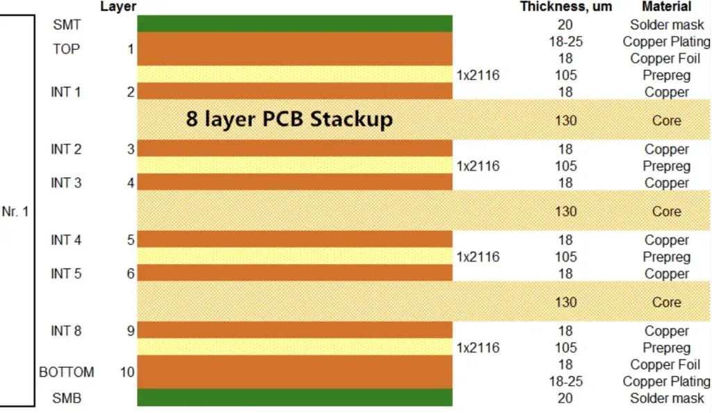
8-Layer PCB Stackup Configurations and Material Impact
The arrangement of layers in an 8-layer PCB stackup is just as important as the material choice. A typical 8-layer stackup might include signal layers, ground planes, and power planes, arranged to minimize crosstalk and ensure stable impedance. Here’s a common configuration:
- Layer 1: Top Signal
- Layer 2: Ground Plane
- Layer 3: Inner Signal
- Layer 4: Power Plane
- Layer 5: Power Plane
- Layer 6: Inner Signal
- Layer 7: Ground Plane
- Layer 8: Bottom Signal
The dielectric material between these layers directly affects signal integrity. For example, in high-frequency designs, using a material with a low Dk ensures consistent impedance across layers, typically targeting 50 ohms for RF traces. If FR-4 is used, the higher Dk can cause impedance mismatches unless trace widths and spacing are carefully calculated. Advanced laminates, with their lower Dk and Df, provide more predictable performance, especially for differential pairs or microstrip lines on outer layers.
8-Layer PCB High-Frequency Materials: When to Upgrade
Not every 8-layer PCB needs high-frequency materials. However, certain applications demand their use to meet performance requirements. Consider upgrading to high-frequency laminates if your design involves:
- High-Speed Signals: Frequencies above 1 GHz, where signal loss and delay become significant with standard materials.
- Impedance-Critical Designs: Applications requiring tight impedance control, such as 50-ohm transmission lines for RF.
- Harsh Environments: High temperatures or humidity that could degrade standard materials like FR-4.
- Miniaturization: Smaller trace widths and spacing, where low Dk materials help maintain signal integrity.
For instance, in a telecommunications board operating at 5 GHz, using a high-frequency laminate with a Dk of 3.0 and Df of 0.002 can reduce signal attenuation by up to 30% compared to FR-4. This directly improves bit error rates and overall system reliability.
8-Layer PCB Dielectric Constant: Fine-Tuning Performance
The dielectric constant of your PCB material isn’t just a number—it’s a key parameter for fine-tuning performance in an 8-layer design. A lower Dk allows for wider traces at the same impedance, which can simplify manufacturing and improve current-carrying capacity. For example, achieving a 50-ohm impedance with a Dk of 4.5 (FR-4) might require a trace width of 0.2 mm, while a Dk of 3.0 could allow a width of 0.3 mm, reducing fabrication challenges.
In multi-layer designs, maintaining a consistent Dk across layers is also critical to avoid signal skew in high-speed digital or RF systems. Variations in Dk between layers can cause timing mismatches, especially for differential signals. When selecting materials, ensure that the core and prepreg layers have matching dielectric properties to maintain uniformity.
8-Layer PCB Material Selection Guide: Step-by-Step
Follow this practical guide to choose the right material for your 8-layer PCB stackup:
- Define Your Frequency Range: Determine if your design operates below 1 GHz (suitable for FR-4) or higher (consider high-frequency laminates).
- Assess Thermal Needs: Check the operating temperature range. If it exceeds 130°C, opt for materials with better thermal stability.
- Evaluate Signal Integrity Requirements: For tight impedance control or low signal loss, prioritize materials with low Dk and Df.
- Consider Budget Constraints: Balance performance with cost. Use FR-4 for non-critical applications to save money.
- Consult with Fabricators: Ensure your chosen material is compatible with standard manufacturing processes to avoid delays or defects.
By following these steps, you can narrow down your options and select a material that aligns with both technical and financial goals.
8-Layer PCB Laminate Comparison: Making the Final Choice
To summarize, the choice between FR-4 and high-frequency laminates for an 8-layer PCB depends on your specific needs. FR-4 offers a cost-effective solution for standard designs, with adequate performance for frequencies below 1 GHz and moderate thermal conditions. High-frequency laminates excel in RF and microwave applications, providing lower signal loss, better impedance stability, and superior thermal management—at a higher cost.
Ultimately, the best material is one that meets your application’s electrical, thermal, and mechanical requirements without exceeding your budget. For mixed-signal designs, hybrid stackups combining FR-4 with high-frequency materials on critical layers can offer a balanced approach, optimizing both cost and performance.
Conclusion: Build Better 8-Layer PCBs with the Right Materials
Designing an 8-layer PCB stackup is a complex task, but choosing the right materials doesn’t have to be. By understanding the impact of dielectric constant, dissipation factor, and thermal stability, you can select a material that ensures reliable performance for your specific application. Whether you stick with the tried-and-true FR-4 or invest in high-frequency laminates for cutting-edge designs, the key is aligning material properties with your project’s needs.
At ALLPCB, we’re committed to helping you navigate these decisions with expert guidance and high-quality manufacturing solutions. With the insights from this guide, you’re well-equipped to build 8-layer PCBs that deliver exceptional results, from concept to completion.


